Wednesday, May 14. 2014
Interfacing Cirrus Logic Audio ADCs
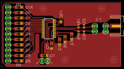
I've been considering ideas for audio gear of various sorts over the past few months, and decided a good starting place would be a solid ADC interface from which I could prototype concepts. Lots of companies make audio converters, but I settled on two models from Cirrus Logic: the CS5361 and CS5340. They are, respectively, balanced and unbalanced two-channel 24-bit 192 khz high dynamic range delta-sigma oversampling devices.
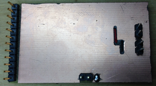
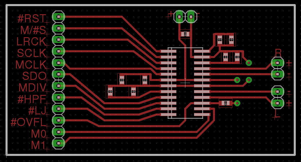
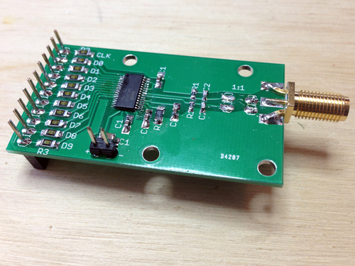
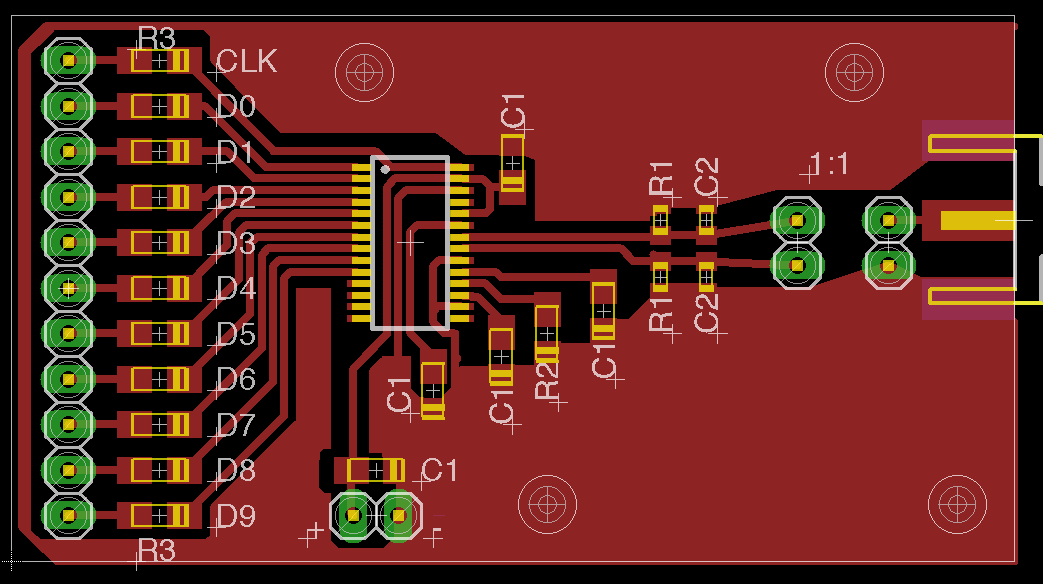
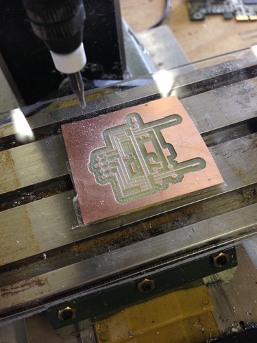
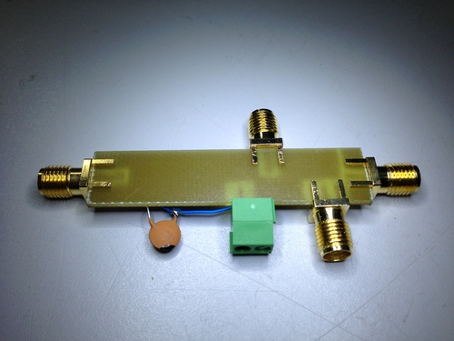
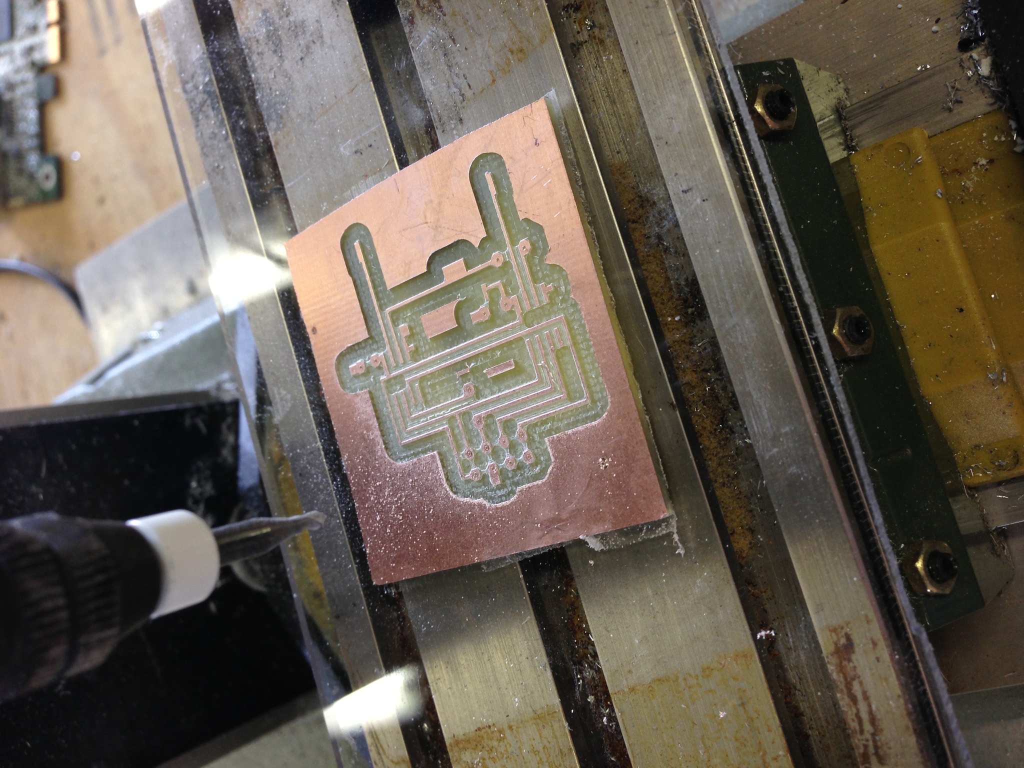
I started by laying out a super-simple protoboard for the CS5361. Since I wanted this to be quick and easy to cut on the CNC mill, the board is single-sided with the bare minimum of filtering, and without standard mixed signal board design concepts like separate analog and digital ground planes. While this will negatively affect the noise figure a bit, I wanted to get the device up and running with the minimum investment of time in case my assumptions regarding its usage and support were incorrect.

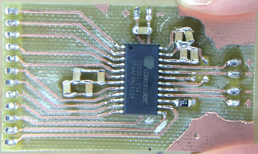
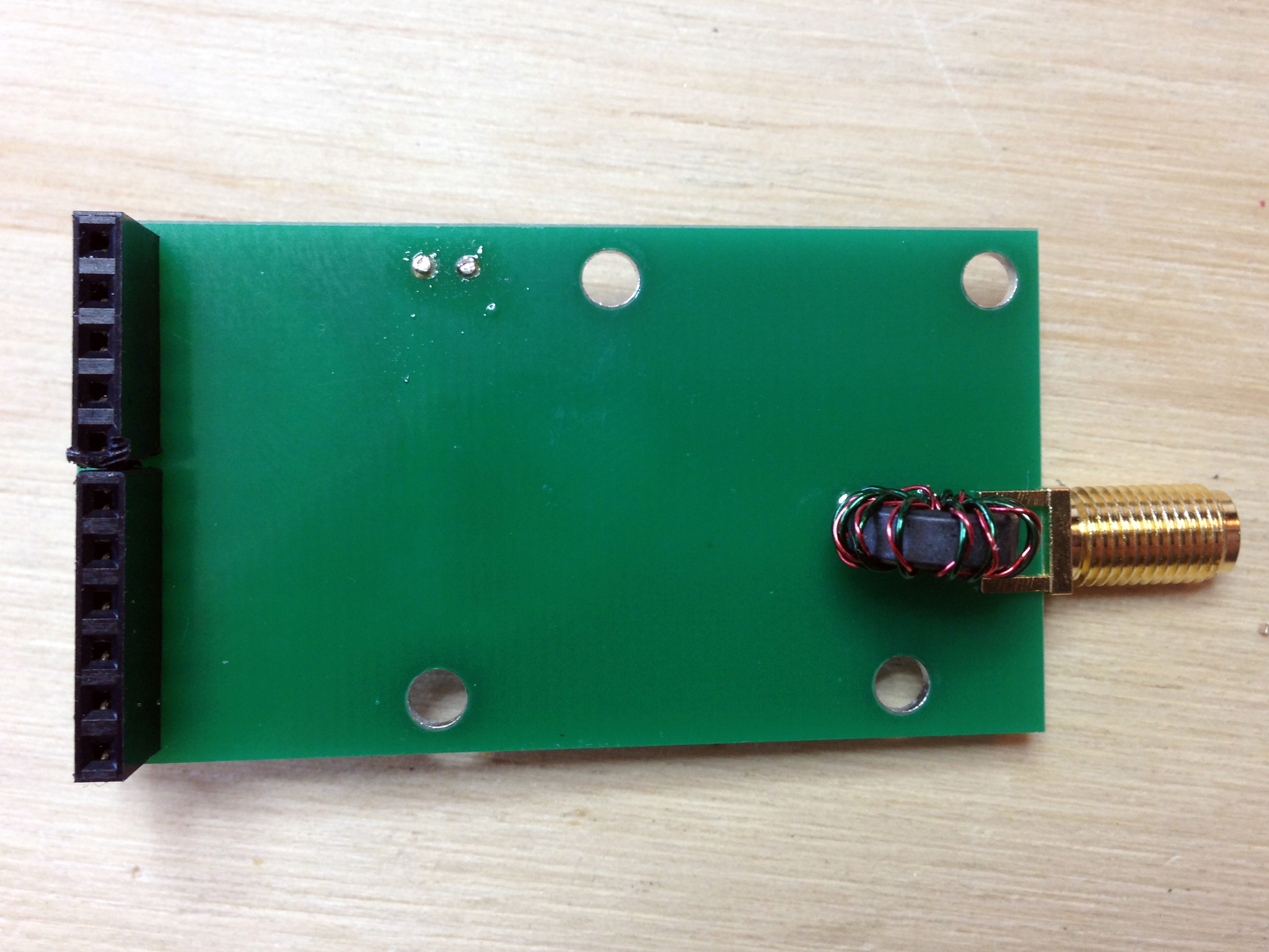
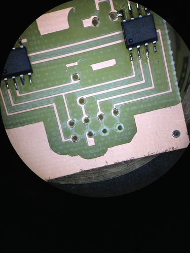
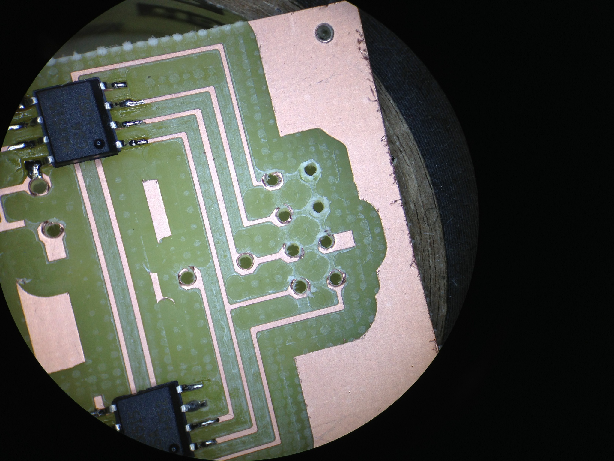
By the time I had finished the layout and cut the board, the samples order had arrived! Soldering was quick though a tad arduous - I need to use a larger 1206 footprint next time.

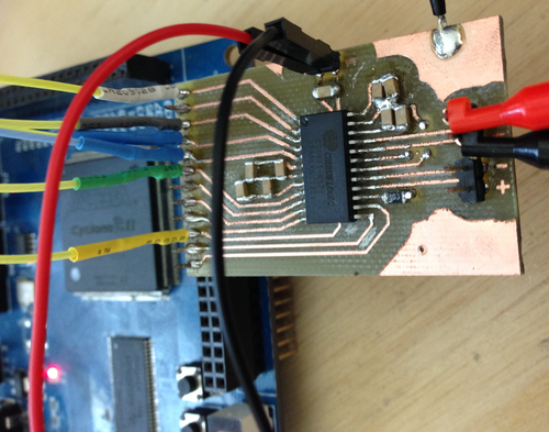
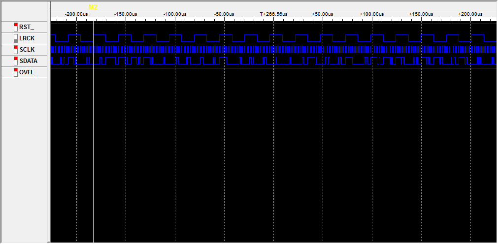
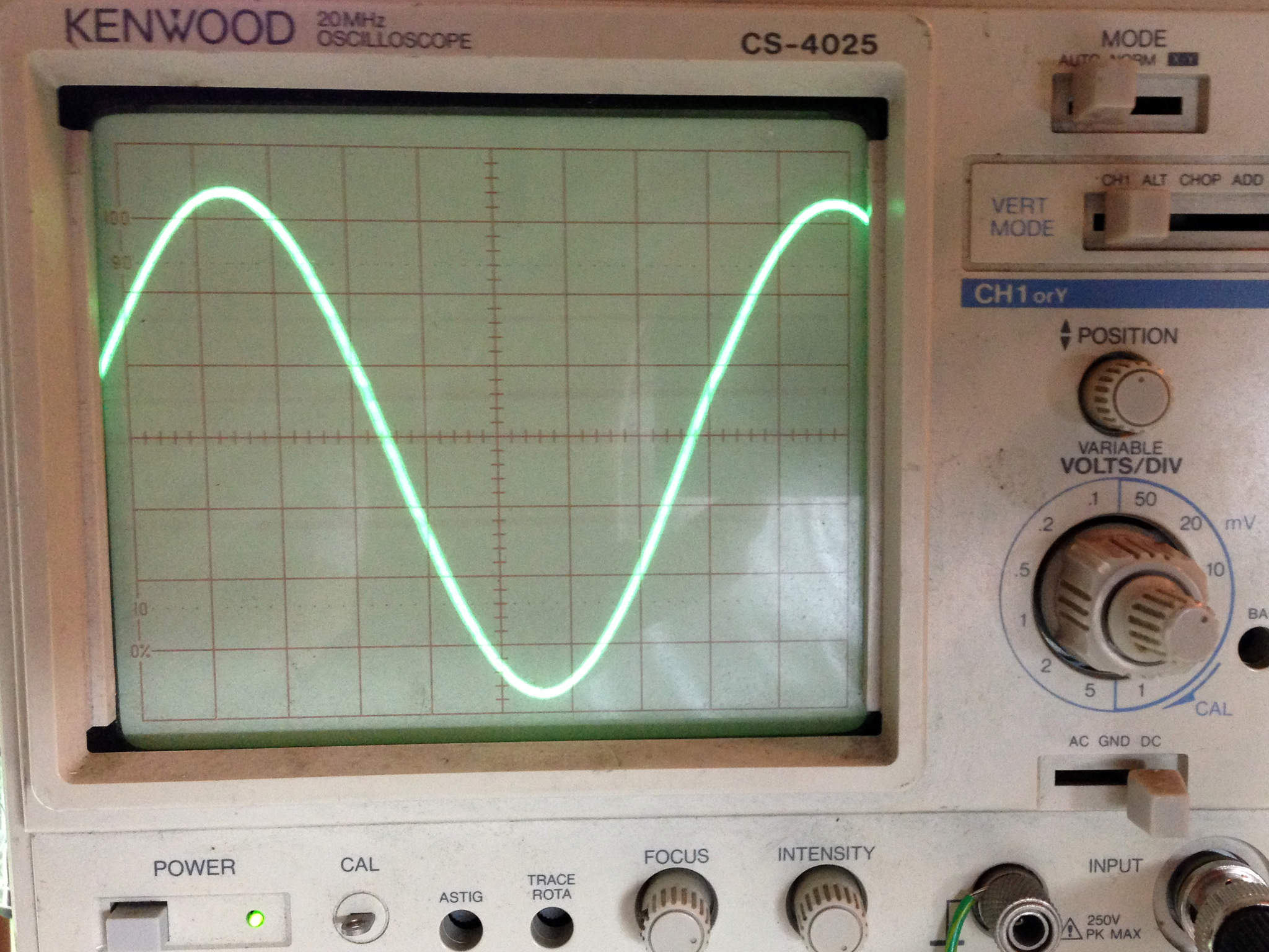
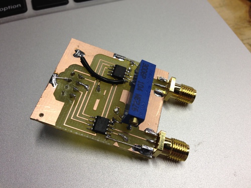
My ugly solder job notwithstanding, I plugged the unit into a breadboard, wired up an oscillator, config pins, and the logic analyzer, and was immediately rewarded with correct operation:
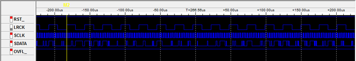
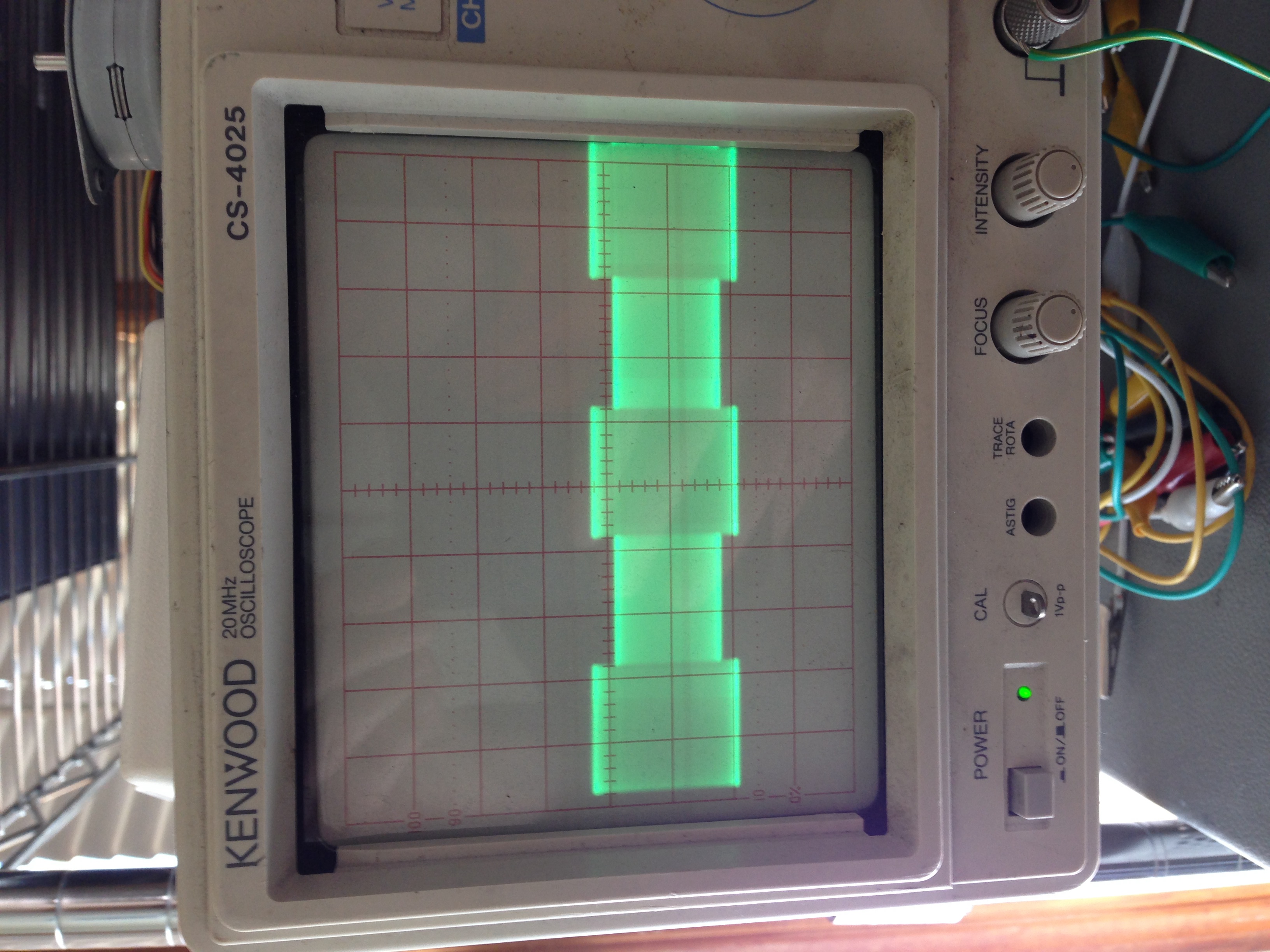
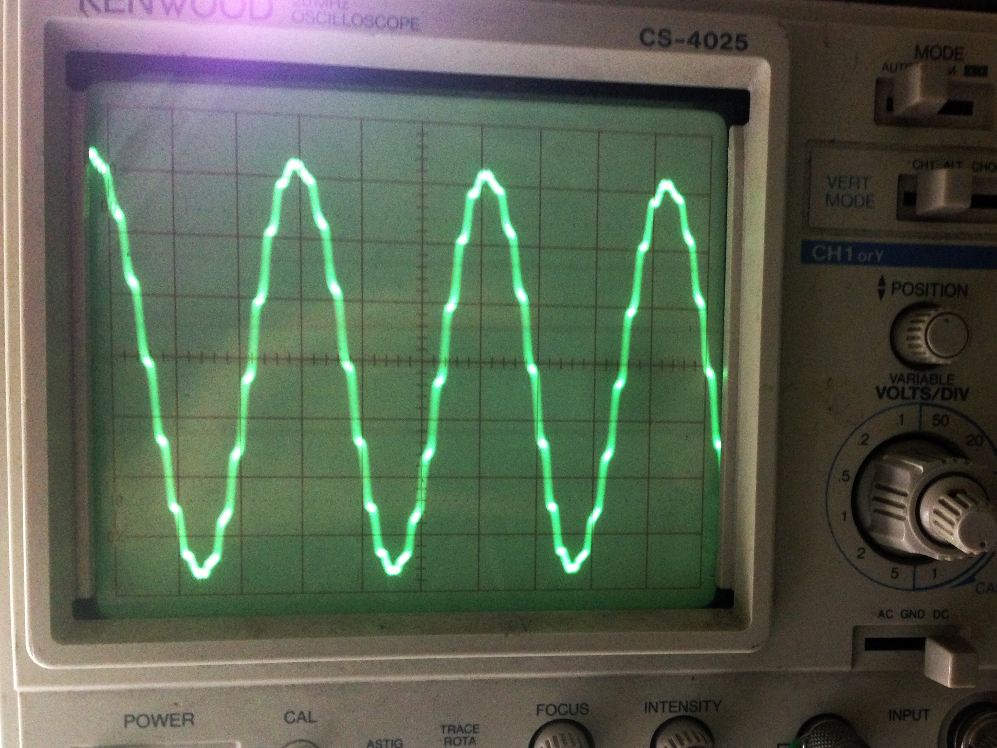
In short, by simply applying power, config pin states, and a master clock, the device will shift out ADC values (in 2's compliment form) msb-first on the falling edge of SCLK (ie, we sample on the rising edge):

The only other line we need to worry about is LRCK, which indicates the channel being sent - you can see here that we get a left sample, then a right sample, then repeat:
With the hardware working, I set about writing the Verilog modules to nab samples from the ADC and send them off via USB (using an FT245R FIFO interface I have on hand). The code is extremely simple: on the rising edge of SCLK, samples are shifted into an 8-bit register - the size of the data bus on the USB interface. Every 8 bits, that register is strobed into the FT245R and the process repeats.
Byte alignment is provided by LRCK: on a start or reset condition from the USB host, the FPGA waits for a rising edge of LRCK before beginning the sampling and transmission of samples. This allows the client end to interpret the data stream without framing bytes: incoming data is simply shifted into 3-byte (24-bit) samples, left then right, and processed as desired.
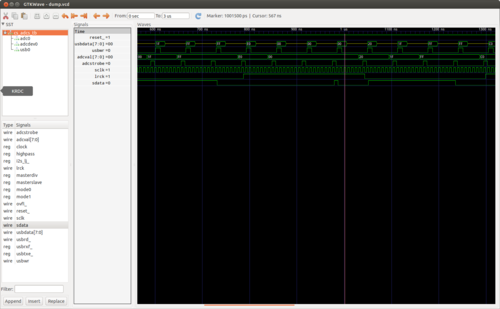
The code was quick to write and simulate with my favorite tools, iVerilog and GTKWave. I implemented a quick CS5361 module whose left and right channels count up and down (respectively) so as to simulate the rest of the pieces. Unfortunately I spent almost as much time debugging the code in hardware with the logic analyzer as I did writing the code, as Quartus (the Altera design software) is rather inconsistent in its handling of constants and register widths. (note: always read every line of output from the Altera synthesis toolchain - one can easily spend 4 hours trying to debug a problem that makes no sense only to find that the synthesis tool decided a constant was the wrong size and used zero instead)
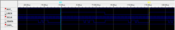
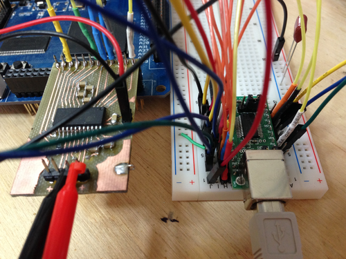
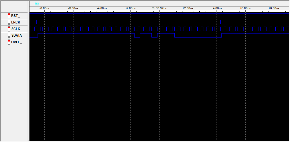
In any event, I did manage to squash the few Quartus oddities that had caused the hardware to operate differently from the simulated code, and verified that the USB interface looked correct using the logic analyzer. Time for more spaghetti:
Time to test it out. In its current state, the FPGA will assert a reset condition on any received byte from the FIFO buffer. So, we will send a reset byte then read 24 samples of 6 bytes (3 for each channel):
root@ichor ~ # echo -n 0 > /dev/ttyUSB0 && dd if=/dev/ttyUSB0 count=24 bs=6 2>/dev/null | hexdump
0000000 3238 a13f 4a68 a650 0344 bd41 6632 ceaa
0000010 78f2 28f8 9764 19ca 7185 45b4 6bfd eabf
0000020 9825 8050 65e5 6122 3adc 0830 28f0 9dfc
0000030 d026 746a e2c0 befa 57dc 1fa4 4225 7b82
0000040 a61b ed00 2320 d641 e111 b648 a2f3 8d3a
0000050 bdfb afb6 1287 5963 ff57 9c8e 63a1 3971
0000060 4bfe ac6e 5081 9fae 2b0d 5c4c 6eaa 26b7
0000070 164b 6093 8378 96d8 138c 160e e661 a81b
0000080 81bc bdae 530b ec79 3537 6ada b0cc 4773
0000090
Success! With that working, the next steps are to implement the CS5340 and add proper dynamic configuration loading. From there, I am hoping to implement ADAT input and output and a simple device driver to interface the kernel audio subsystem.
I've put the code, board design, and a bit of documentation on GitHub: jackcarrozzo/cs_adcs.
I started by laying out a super-simple protoboard for the CS5361. Since I wanted this to be quick and easy to cut on the CNC mill, the board is single-sided with the bare minimum of filtering, and without standard mixed signal board design concepts like separate analog and digital ground planes. While this will negatively affect the noise figure a bit, I wanted to get the device up and running with the minimum investment of time in case my assumptions regarding its usage and support were incorrect.
By the time I had finished the layout and cut the board, the samples order had arrived! Soldering was quick though a tad arduous - I need to use a larger 1206 footprint next time.

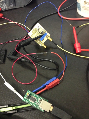
My ugly solder job notwithstanding, I plugged the unit into a breadboard, wired up an oscillator, config pins, and the logic analyzer, and was immediately rewarded with correct operation:
In short, by simply applying power, config pin states, and a master clock, the device will shift out ADC values (in 2's compliment form) msb-first on the falling edge of SCLK (ie, we sample on the rising edge):
The only other line we need to worry about is LRCK, which indicates the channel being sent - you can see here that we get a left sample, then a right sample, then repeat:

With the hardware working, I set about writing the Verilog modules to nab samples from the ADC and send them off via USB (using an FT245R FIFO interface I have on hand). The code is extremely simple: on the rising edge of SCLK, samples are shifted into an 8-bit register - the size of the data bus on the USB interface. Every 8 bits, that register is strobed into the FT245R and the process repeats.
Byte alignment is provided by LRCK: on a start or reset condition from the USB host, the FPGA waits for a rising edge of LRCK before beginning the sampling and transmission of samples. This allows the client end to interpret the data stream without framing bytes: incoming data is simply shifted into 3-byte (24-bit) samples, left then right, and processed as desired.

The code was quick to write and simulate with my favorite tools, iVerilog and GTKWave. I implemented a quick CS5361 module whose left and right channels count up and down (respectively) so as to simulate the rest of the pieces. Unfortunately I spent almost as much time debugging the code in hardware with the logic analyzer as I did writing the code, as Quartus (the Altera design software) is rather inconsistent in its handling of constants and register widths. (note: always read every line of output from the Altera synthesis toolchain - one can easily spend 4 hours trying to debug a problem that makes no sense only to find that the synthesis tool decided a constant was the wrong size and used zero instead)

In any event, I did manage to squash the few Quartus oddities that had caused the hardware to operate differently from the simulated code, and verified that the USB interface looked correct using the logic analyzer. Time for more spaghetti:

Time to test it out. In its current state, the FPGA will assert a reset condition on any received byte from the FIFO buffer. So, we will send a reset byte then read 24 samples of 6 bytes (3 for each channel):
root@ichor ~ # echo -n 0 > /dev/ttyUSB0 && dd if=/dev/ttyUSB0 count=24 bs=6 2>/dev/null | hexdump
0000000 3238 a13f 4a68 a650 0344 bd41 6632 ceaa
0000010 78f2 28f8 9764 19ca 7185 45b4 6bfd eabf
0000020 9825 8050 65e5 6122 3adc 0830 28f0 9dfc
0000030 d026 746a e2c0 befa 57dc 1fa4 4225 7b82
0000040 a61b ed00 2320 d641 e111 b648 a2f3 8d3a
0000050 bdfb afb6 1287 5963 ff57 9c8e 63a1 3971
0000060 4bfe ac6e 5081 9fae 2b0d 5c4c 6eaa 26b7
0000070 164b 6093 8378 96d8 138c 160e e661 a81b
0000080 81bc bdae 530b ec79 3537 6ada b0cc 4773
0000090
Success! With that working, the next steps are to implement the CS5340 and add proper dynamic configuration loading. From there, I am hoping to implement ADAT input and output and a simple device driver to interface the kernel audio subsystem.
I've put the code, board design, and a bit of documentation on GitHub: jackcarrozzo/cs_adcs.
Tuesday, February 25. 2014
FPGA Dual DAC Board for QAM Synthesis
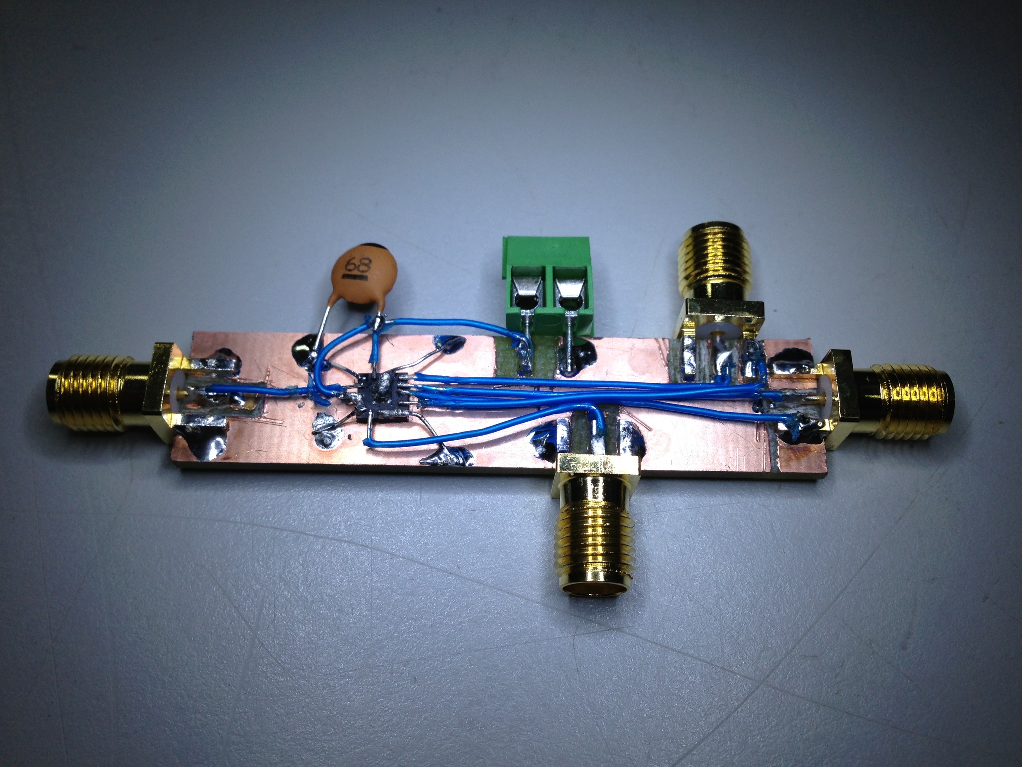
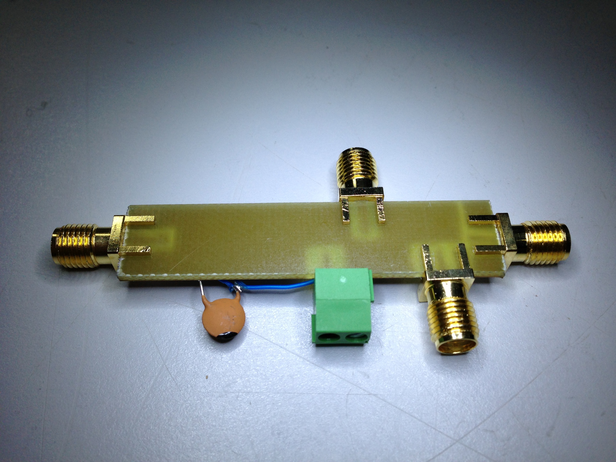
Building on the simplicity and success of my DAC board paired with my FPGA dev boards, today I threw together a board with an Altera Cyclone II, two DAC9000Es, an FT245R, and supporting periphery. I'll need to check it with fresh eyes tomorrow to ensure I haven't made any mistakes, but with luck I can submit the design tomorrow evening and have the boards next week.
My DAC+FPGA pair has proved extremely useful for transmitting test signals of various sorts, taking I+Q via USB and generating the output signal in code. But, at 160 MS/s, its max frequency is quite limited. This new board has two of the same DACs, however each will simply generate the I or Q signal alone which will then be combined with an LO in a dedicated QAM modulator chip. This allows for carrier frequencies limited only by the abilities of the QAM modulator chosen, and at 160 MS/s the usable Tx bandwidth will be huge.
I've chosen to terminate the DACs in SMA connectors and leave the modulator off the board entirely, as I'd like to evaluate a few different chips. Unfortunately this board will be too large for me to mill at home at the moment, but I can still quickly mill test boards for QAM modulators in about an hour.
Thursday, February 20. 2014
WWVB Receiver and Testing Transmitter
As I've been making steady progress on my Z80 computer, I've put a lot of thought into something to actually do with it when it's done. As tempting as it is to load up CP/M, add a video interface, and use it as my main machine, I think porting Firefox is too ambitious. For now, I've decided to add some more 7-segment displays and an RF front end to decode the WWVB time signal from an atomic clock in Colorado and hang it on the wall. If I'm still feeling ambitious, I'll add an Ethernet controller and write a driver and NTP daemon for it. Of course, this means I need a working receiver front end for 60kHz.

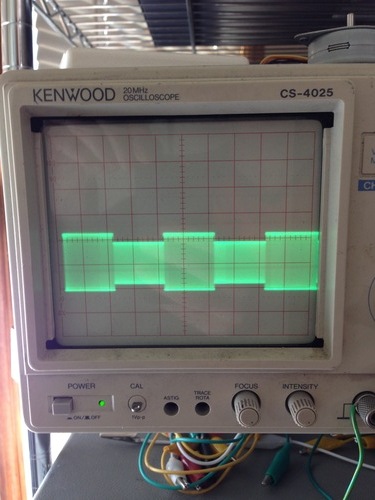
The WWVB signal is quite simple as far as decoding goes: the carrier has "full power" and "low power" states. The transmitter drops the carrier by 17 dB at the start of each second, and the length of time before it returns provides a single trinary value: Mark (0.8s), Not Set (0.2s), or Set (0.5s). A single digital line that goes low or high to follow the transmitter power state is quite easy to achieve with a fully analog circuit: after a bandpass to select only the 60kHz carrier, we send the signal into two peak detectors - one with a long time constant (low pass filter) to track the average signal power over several seconds, and one with a shorter time constant to track the per-second changes. Passing these two signals to a comparator, we get our nice single-bit TTL indicator of the current signal state. Plus, the longer time constant peak detector acts as an auto gain control, so no alignment is required.

While I will make my own receiver as described above for the final version, I ordered a SYM-RFT module for testing. It includes an LED to indicate received carrier status and outputs the inverted carrier power state compared to the average carrier power. I quickly breadboarded it up to an FT245R USB chip and wrote a few lines of C to poll the power status and measure the length of state changes. Unfortunately, New England being quite far from Colorado, the signal is below the noise floor and has thus far been highly unreliable. The module simply flashes chaotically in the presence of any electronic noise like my monitors, and does nothing in isolation.
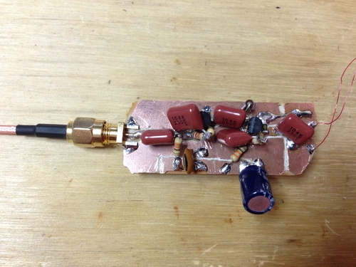
I built the above two-stage preamp from two 2N3904's to attach to the 60kHz antenna that came with the SYM-RFT module to see if I could see any carrier on the oscilloscope. While I did get all sorts of noise and impulses, there was very little if any energy at 60kHz. Drat.
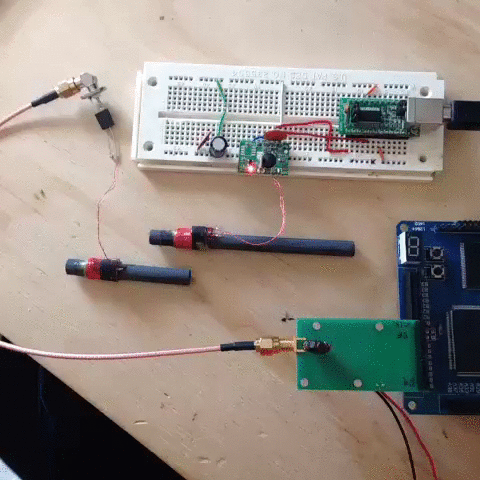
Luckily, I have the tools on hand to recreate the signal so I can at least test my receiver and code. I pulled out the FPGA RF DAC board I put together a while back, and a page of Verilog later I had a compliant WWVB transmitter:
After a small battle with PLLs to get a slow enough clock for 60khz, both the SYM-RFT and my USB worked fine.
jackc@ichor ~/Projects/wwvb_usb $ sudo ./wwvb
MARK : 950 ms
NOT SET : 239 ms
SET : 503 ms
NOT SET : 194 ms
SET : 581 ms
MARK : 991 ms
^Cjackc@ichor ~/Projects/wwvb_usb $
The WWVB signal is quite simple as far as decoding goes: the carrier has "full power" and "low power" states. The transmitter drops the carrier by 17 dB at the start of each second, and the length of time before it returns provides a single trinary value: Mark (0.8s), Not Set (0.2s), or Set (0.5s). A single digital line that goes low or high to follow the transmitter power state is quite easy to achieve with a fully analog circuit: after a bandpass to select only the 60kHz carrier, we send the signal into two peak detectors - one with a long time constant (low pass filter) to track the average signal power over several seconds, and one with a shorter time constant to track the per-second changes. Passing these two signals to a comparator, we get our nice single-bit TTL indicator of the current signal state. Plus, the longer time constant peak detector acts as an auto gain control, so no alignment is required.
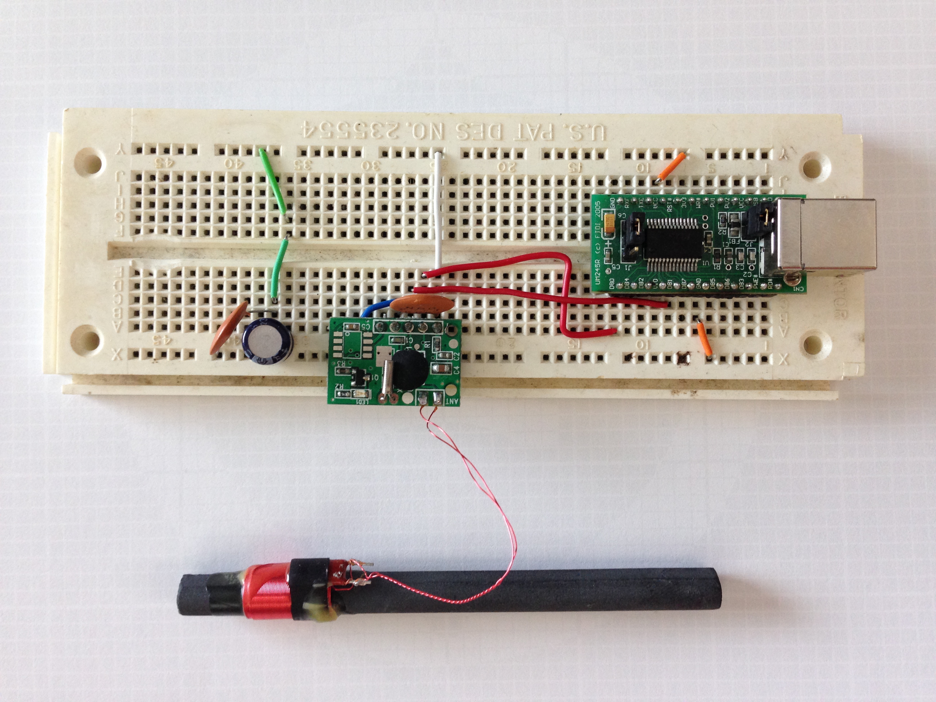
While I will make my own receiver as described above for the final version, I ordered a SYM-RFT module for testing. It includes an LED to indicate received carrier status and outputs the inverted carrier power state compared to the average carrier power. I quickly breadboarded it up to an FT245R USB chip and wrote a few lines of C to poll the power status and measure the length of state changes. Unfortunately, New England being quite far from Colorado, the signal is below the noise floor and has thus far been highly unreliable. The module simply flashes chaotically in the presence of any electronic noise like my monitors, and does nothing in isolation.
I built the above two-stage preamp from two 2N3904's to attach to the 60kHz antenna that came with the SYM-RFT module to see if I could see any carrier on the oscilloscope. While I did get all sorts of noise and impulses, there was very little if any energy at 60kHz. Drat.
Luckily, I have the tools on hand to recreate the signal so I can at least test my receiver and code. I pulled out the FPGA RF DAC board I put together a while back, and a page of Verilog later I had a compliant WWVB transmitter:
After a small battle with PLLs to get a slow enough clock for 60khz, both the SYM-RFT and my USB worked fine.
jackc@ichor ~/Projects/wwvb_usb $ sudo ./wwvb
MARK : 950 ms
NOT SET : 239 ms
SET : 503 ms
NOT SET : 194 ms
SET : 581 ms
MARK : 991 ms
^Cjackc@ichor ~/Projects/wwvb_usb $
Tuesday, February 11. 2014
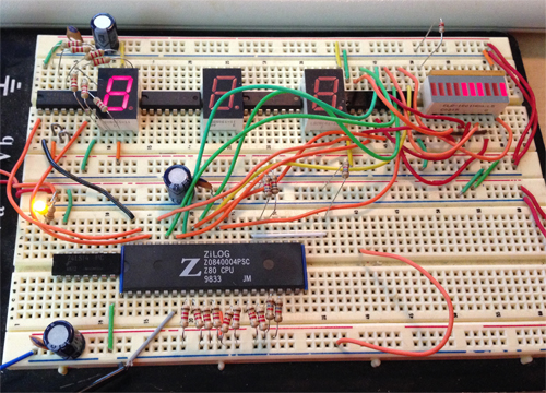
Z80 Proto Coming Along Nicely
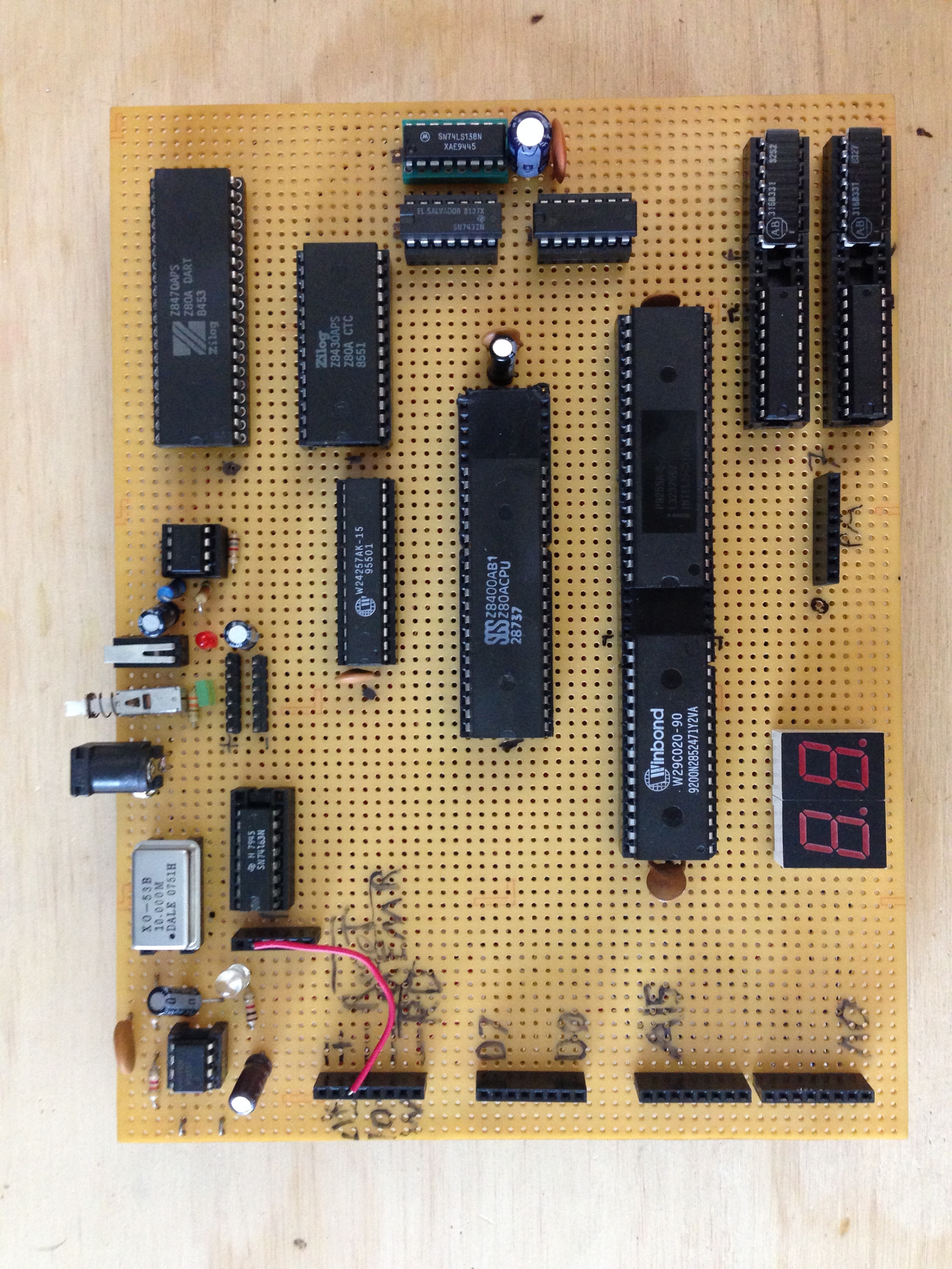
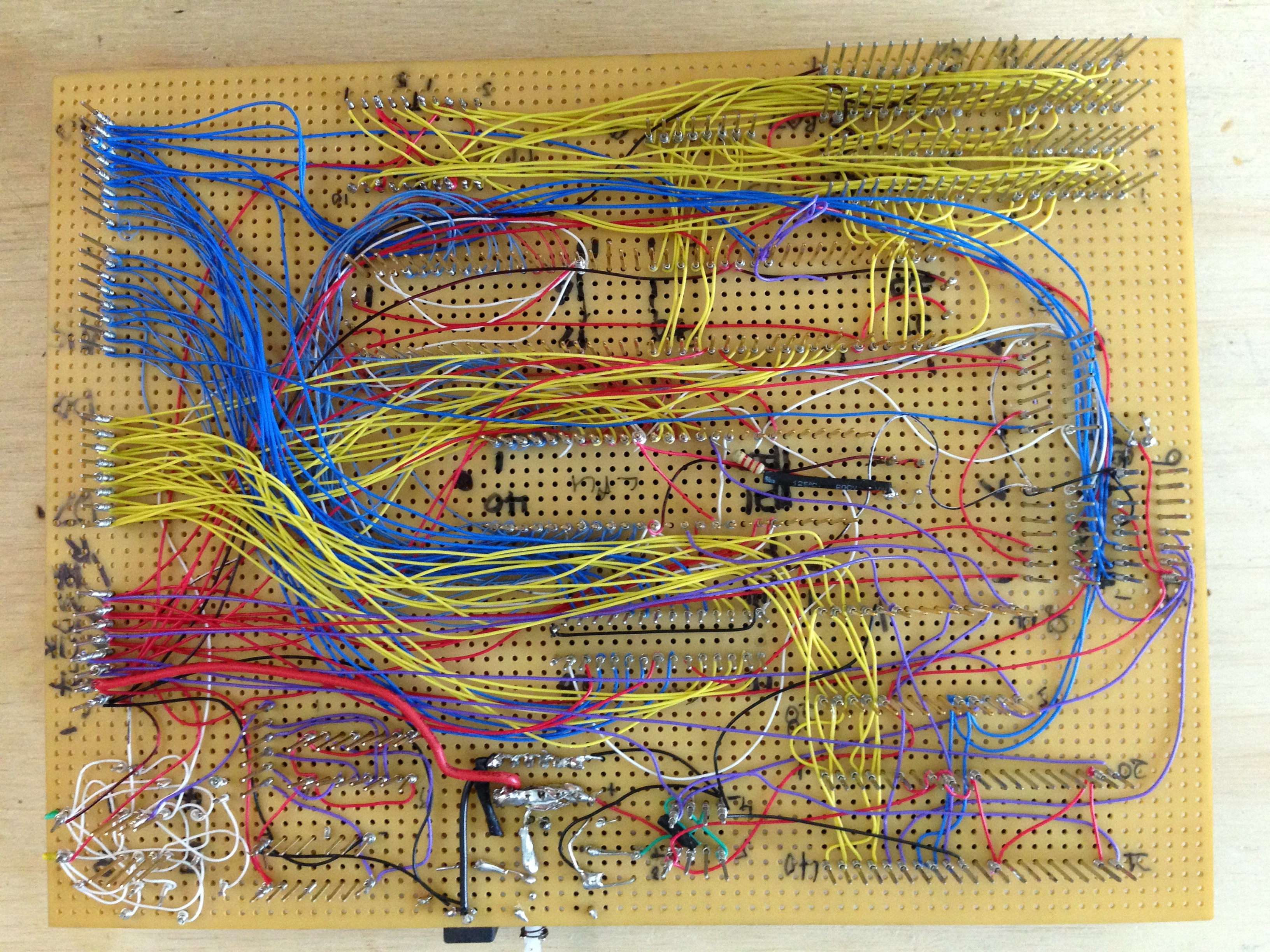
I've rebuilt my previous Z80 computer and have been adding several peripherals of late. I think that ultimatly, after I decide the final design, I'll rebuild the whole thing to look pretty and be better laid out for higher clock speeds, but for now I'm continuing to prototype here.
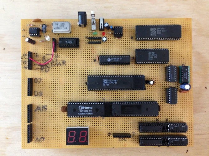
As it stands, I have the following systems configured:
CPU: Z80A - While I have some later devices with more features and faster clocks on hand, I'm testing base functionality with a run-of-the-mill original.
Flash: W29C020 - Boot ROM. The device is 256 kB, but I'm only using 32k (memory map is split between RAM and ROM). Technically I could enable write functionality to the flash, but haven't done so thus far as I haven't needed it.
SRAM: W24257AK - 32k. Haven't implemented any MMU or paging, but it would be trivial to do so in the future if need be.
Address Decoding and Glue: 74LS138, 74LS32, 74LS04 - Some people use PLAs or GALs to do this in a single device, but I have an attachment 7400 series logic.
General Purpose IO: 8255A - Provides three 8-bit ports per chip. Right now ports A and B are tied to 7-segment displays via 74LS244 octal buffers. Rather than use 7447 7-segment decoders to save 4 bits, I connected the displays directly so that I can display the A-F characters correctly via a map in ROM. This has been quite helpful while writing the BIOS.
Timing: Z8430APS CTC - This guy provides four counter channels with a handy list of prescalers and vectored interrupt features. Right now the BIOS configures channel 0 to send an interrupt every 10ms for polling routines, and channel 1 to provide a compatible baud rate clock to the DART.
Async Serial: Z8470APS DART - Contains a whole slew of serial comm features. Currently the BIOS configures channel A for 9600 8N1 and transmits debugging information through it.
System Clock: 10MHz Osc + 74LS163 Counter - The 4-bit counter provides clocks at 5, 2.5, 1.25, and 0.625 MHz, selectable via pin header. The 555 in the upper-left corner provides a 10kHz clock signal for visual debugging also, but at this point the BIOS is far too long to sit around waiting for it to boot at that clock speed.
Reset Controller: Analog! - At power on, a 1uF capacitor is slowly filled through a 1Mohm resistor to Vcc. When its voltage exceeds that set be a voltage divider (1/2 Vcc here), a comparator (TLC3702) releases the RESET_ assertion. A switch between ground and the capacitor provides another way to trigger a reset.

So far so good! Hopefully I don't jinx myself here, but I haven't made a single wiring mistake yet. I have the logic analyzer sitting here ready, but every time I've added a new chip the unit has just booted right up and worked flawlessly - I can't believe it, given the sheer number of connections.
By the way, I forked the assembler and fixed a few tiny things. Check it out on GitHub: z80asm. Also, I've spent a good bit of time writing emulations of the 8255, CTC, and DART in C as well as fixing the interrupt handling in my fork of z80sim: see my fork here. The file containing the my chip emulations is io.c (a work in progress at the time of writing).
As it stands, I have the following systems configured:
CPU: Z80A - While I have some later devices with more features and faster clocks on hand, I'm testing base functionality with a run-of-the-mill original.
Flash: W29C020 - Boot ROM. The device is 256 kB, but I'm only using 32k (memory map is split between RAM and ROM). Technically I could enable write functionality to the flash, but haven't done so thus far as I haven't needed it.
SRAM: W24257AK - 32k. Haven't implemented any MMU or paging, but it would be trivial to do so in the future if need be.
Address Decoding and Glue: 74LS138, 74LS32, 74LS04 - Some people use PLAs or GALs to do this in a single device, but I have an attachment 7400 series logic.
General Purpose IO: 8255A - Provides three 8-bit ports per chip. Right now ports A and B are tied to 7-segment displays via 74LS244 octal buffers. Rather than use 7447 7-segment decoders to save 4 bits, I connected the displays directly so that I can display the A-F characters correctly via a map in ROM. This has been quite helpful while writing the BIOS.
Timing: Z8430APS CTC - This guy provides four counter channels with a handy list of prescalers and vectored interrupt features. Right now the BIOS configures channel 0 to send an interrupt every 10ms for polling routines, and channel 1 to provide a compatible baud rate clock to the DART.
Async Serial: Z8470APS DART - Contains a whole slew of serial comm features. Currently the BIOS configures channel A for 9600 8N1 and transmits debugging information through it.
System Clock: 10MHz Osc + 74LS163 Counter - The 4-bit counter provides clocks at 5, 2.5, 1.25, and 0.625 MHz, selectable via pin header. The 555 in the upper-left corner provides a 10kHz clock signal for visual debugging also, but at this point the BIOS is far too long to sit around waiting for it to boot at that clock speed.
Reset Controller: Analog! - At power on, a 1uF capacitor is slowly filled through a 1Mohm resistor to Vcc. When its voltage exceeds that set be a voltage divider (1/2 Vcc here), a comparator (TLC3702) releases the RESET_ assertion. A switch between ground and the capacitor provides another way to trigger a reset.
So far so good! Hopefully I don't jinx myself here, but I haven't made a single wiring mistake yet. I have the logic analyzer sitting here ready, but every time I've added a new chip the unit has just booted right up and worked flawlessly - I can't believe it, given the sheer number of connections.
By the way, I forked the assembler and fixed a few tiny things. Check it out on GitHub: z80asm. Also, I've spent a good bit of time writing emulations of the 8255, CTC, and DART in C as well as fixing the interrupt handling in my fork of z80sim: see my fork here. The file containing the my chip emulations is io.c (a work in progress at the time of writing).
Tuesday, January 14. 2014
Z80 Computer and Assembler Adventures
I recently pulled out the Z80 project computer I built several years ago in the hopes of adding some hardware and features to it, but was sad to find that it didn't want to operate in the slightest. A quick connection of the logic analyzer showed that the CPU was not fetching instructions. Hrm. I needed to determine if my delicate, hand-wired little computer was at fault somewhere, or if the CPU itself was upset.
First, I breadboarded the following setup to test the Z80. Since the opcode for the NOP instruction is 0x00, setting the data bus to zeros and providing correct external state causes the chip to simply count up the address bus when clocked. I pulled the data bus to 0s with 1k resistors since the chip is in an undefined state before reset and could attempt to write to the bus - bad news if you're tied to a rail. I then set WAIT_, INT_, NMI_, and BUSREQ_, leaving just a RESET_ and a clock source to add.
I really like the simplicity of Z80: not only can I run the chip with only four pullups and no external components, but it will run with clock speeds all the way down to DC. That means you can single step your computer with a debounced push button as your clock - try that on a modern CPU! For this particular exercise, I rigged a 555 timer to generate a 10hz clock - slow enough to watch the address bus with LEDs.
At the moment of truth, I got... nothing. The chip was tri-stating the address bus and not responding to RESET_. Unfortunately this meant I needed to dig deep into the depths to locate my box of Z80 items that I hadn't seen since college. However, not only did I find the box I was looking for quite quickly, I found a downright awesome pile of parts in there! I recalled that I had 3 extra Z80s and two 82C55's, but in reality I owned 16 Z80s of different vintages and speed grades, a few different types of 82C55, and an awesome pile of Z84 family peripheral controllers. I was very pleased.
Back at my desk, I tested all 17 CPUs (the one that was in my computer, plus the 16 extra ones I had). It turns out that all of my spares are in perfect working condition, and the one in the computer was in fact dead as a door nail. Good to know!
Next, I put a working CPU back in the computer, then wrote, assembled (using z80asm-1.2), and burned the following test program into flash:
LD A,0x80 ; 1000 0000 - tell the 82C55 to set all ports to outputs
OUT (3),A ; 0x03 is the control word address
LD A,1 ; set one bit that we will rotate in the loop
loop: OUT (0),A ; put the word out on port A of the 82C55
NOP
RLCA ; left-rotate reg A
JP loop
Sure enough, it worked great in hardware. Unfortunately, I decided to test the code in an emulator before running the hardware, and ended up spending many hours debugging and rewriting the emulator's memory loading functionality to be properly endian-safe and to autodetect binary blob types, but I'll leave that rant for another time. In any event, this was a great refresher in Z80 architecture and assembly as well as the interworkings of the emulator. Now that my Z80 computer is working, I have no excuse not to add more cool things to the project...
First, I breadboarded the following setup to test the Z80. Since the opcode for the NOP instruction is 0x00, setting the data bus to zeros and providing correct external state causes the chip to simply count up the address bus when clocked. I pulled the data bus to 0s with 1k resistors since the chip is in an undefined state before reset and could attempt to write to the bus - bad news if you're tied to a rail. I then set WAIT_, INT_, NMI_, and BUSREQ_, leaving just a RESET_ and a clock source to add.
I really like the simplicity of Z80: not only can I run the chip with only four pullups and no external components, but it will run with clock speeds all the way down to DC. That means you can single step your computer with a debounced push button as your clock - try that on a modern CPU! For this particular exercise, I rigged a 555 timer to generate a 10hz clock - slow enough to watch the address bus with LEDs.

At the moment of truth, I got... nothing. The chip was tri-stating the address bus and not responding to RESET_. Unfortunately this meant I needed to dig deep into the depths to locate my box of Z80 items that I hadn't seen since college. However, not only did I find the box I was looking for quite quickly, I found a downright awesome pile of parts in there! I recalled that I had 3 extra Z80s and two 82C55's, but in reality I owned 16 Z80s of different vintages and speed grades, a few different types of 82C55, and an awesome pile of Z84 family peripheral controllers. I was very pleased.
Back at my desk, I tested all 17 CPUs (the one that was in my computer, plus the 16 extra ones I had). It turns out that all of my spares are in perfect working condition, and the one in the computer was in fact dead as a door nail. Good to know!
Next, I put a working CPU back in the computer, then wrote, assembled (using z80asm-1.2), and burned the following test program into flash:
LD A,0x80 ; 1000 0000 - tell the 82C55 to set all ports to outputs
OUT (3),A ; 0x03 is the control word address
LD A,1 ; set one bit that we will rotate in the loop
loop: OUT (0),A ; put the word out on port A of the 82C55
NOP
RLCA ; left-rotate reg A
JP loop
Sure enough, it worked great in hardware. Unfortunately, I decided to test the code in an emulator before running the hardware, and ended up spending many hours debugging and rewriting the emulator's memory loading functionality to be properly endian-safe and to autodetect binary blob types, but I'll leave that rant for another time. In any event, this was a great refresher in Z80 architecture and assembly as well as the interworkings of the emulator. Now that my Z80 computer is working, I have no excuse not to add more cool things to the project...
Tuesday, October 22. 2013
Gyro-Stabilized DSLR Platform
I finally had time to put together one axis of my DSLR gyro frame today, and I am quite pleased with the results. The frame is big and heavy as it was originally intended to be a fixed-mount azimuth-altitude star and satellite rig for taking long exposures of planets and orbiting things, but it happened to be a good test bed for my gyro code. It's rock solid thus far:
Hopefully I will find time to build another axis soon so I can really see how solid both my math and my sensor are. I have a huge list of epic features to add to the project, too. I'm hoping I can get it solid enough to film with a 300mm lens and not need post-process stabilization.

Hopefully I will find time to build another axis soon so I can really see how solid both my math and my sensor are. I have a huge list of epic features to add to the project, too. I'm hoping I can get it solid enough to film with a 300mm lens and not need post-process stabilization.
Tuesday, June 4. 2013
FPGA QAM Generation
I recently drew up a board to connect a fast DAC to FPGA dev boards for the purpose of RF generation. I chose the DAC900E from TI as it's fast (165MS/s), pretty accurate (10-bit), and extremely easy to interface (latches values in on clock edges, doesn't require any setup or external stuff).
Normally I'd cut a simple one-layer board like this on my CNC mill, but I wanted to try a low cost hobbyist PCB fab I read about via Sparkfun. The did take a very long while, but came out beautifully. Also, when the boards finally arrived, I was pleased I had picked a DAC with so few external requirements to solder. The resistors are there to prevent an output buffer short in case I soldered badly, by the way - I don't own a hot air rework setup.

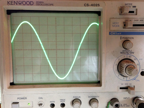
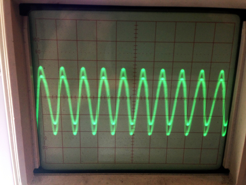
Right off the bat, I was pleased to see that my sine-generation test code worked great at various frequencies and bit depths (aliasing visible in the 2nd pic, its harmonics in the 3rd):


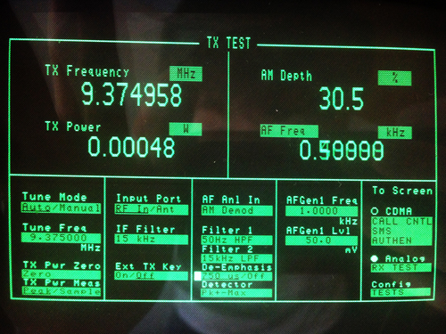
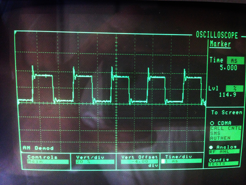
With a bit more hacking, I got the FT245R interface to work such that I send I and Q values via USB, the output value is calculated from an LUT (I originally was doing the math out, but hardware multiply is very slow), and sent to the DAC. In these pics, you can see that I was generating a 500-hz tone over an AM carrier at 9.375 MHz (the 3rd image is the AM-demodulated signal shown on the spectrum analyzer).
My code is on Github here. It's by no means robust or feature-rich, but it does work well in my opinion. When I have time, I'd like to see how far I can take this design. Assuming I don't find any unforseen roadblocks, the next step will be to make a board with two DAC900Es for I and Q generation that feed into a GHz-range QAM modulator that takes its carrier from a PLL on the FPGA, which will theoretically give me full TX control over a wide range of freqs.
Normally I'd cut a simple one-layer board like this on my CNC mill, but I wanted to try a low cost hobbyist PCB fab I read about via Sparkfun. The did take a very long while, but came out beautifully. Also, when the boards finally arrived, I was pleased I had picked a DAC with so few external requirements to solder. The resistors are there to prevent an output buffer short in case I soldered badly, by the way - I don't own a hot air rework setup.

Right off the bat, I was pleased to see that my sine-generation test code worked great at various frequencies and bit depths (aliasing visible in the 2nd pic, its harmonics in the 3rd):
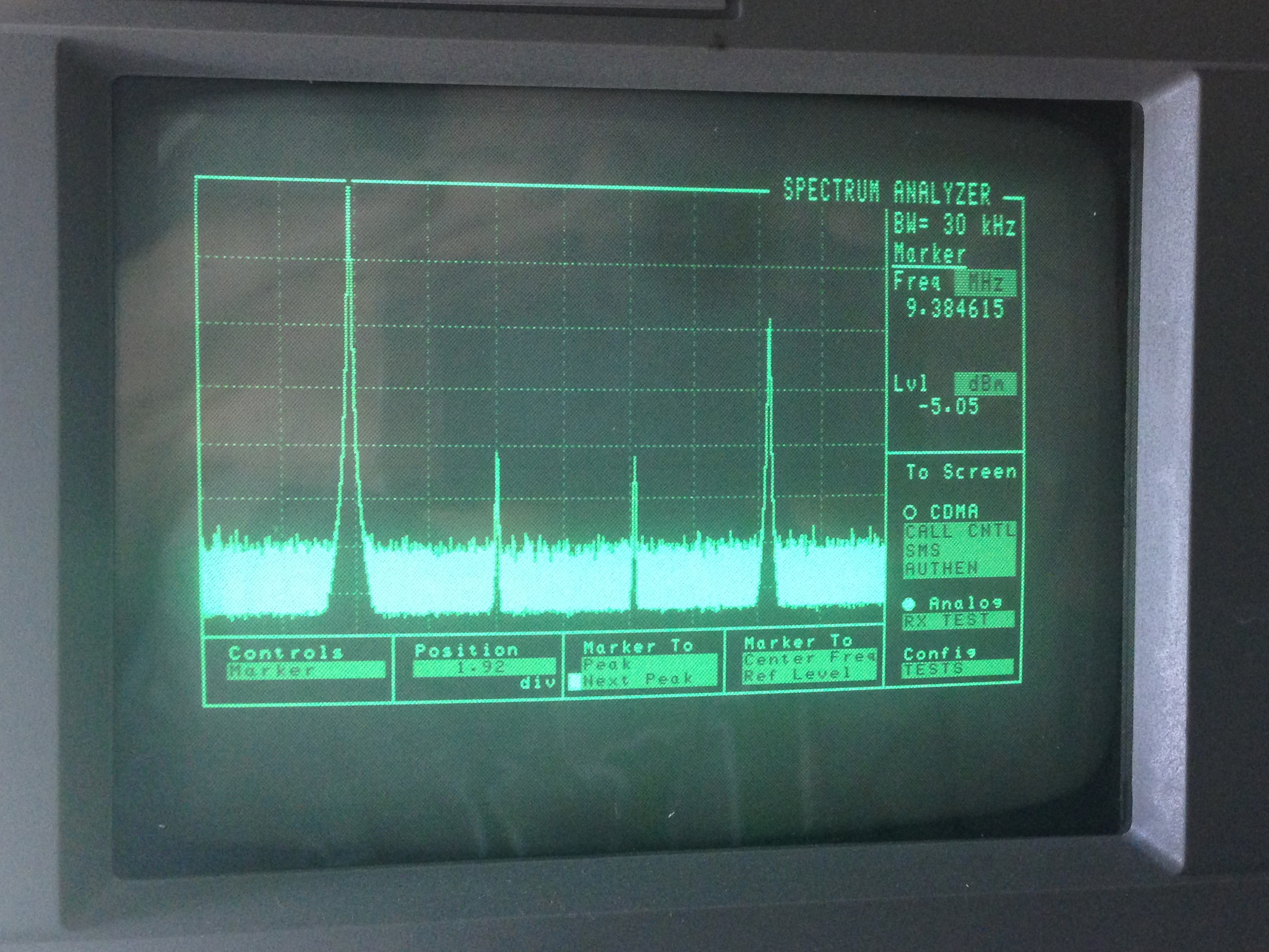
With a bit more hacking, I got the FT245R interface to work such that I send I and Q values via USB, the output value is calculated from an LUT (I originally was doing the math out, but hardware multiply is very slow), and sent to the DAC. In these pics, you can see that I was generating a 500-hz tone over an AM carrier at 9.375 MHz (the 3rd image is the AM-demodulated signal shown on the spectrum analyzer).


My code is on Github here. It's by no means robust or feature-rich, but it does work well in my opinion. When I have time, I'd like to see how far I can take this design. Assuming I don't find any unforseen roadblocks, the next step will be to make a board with two DAC900Es for I and Q generation that feed into a GHz-range QAM modulator that takes its carrier from a PLL on the FPGA, which will theoretically give me full TX control over a wide range of freqs.
Sunday, January 6. 2013
Dual DAC I+Q Generation and Carrier Modulation
I wanted a simple, easily-interfacable QAM source to test some code I had written for the RTL-SDR, so I put together two small boards: one with two SPI DACs to generate the I and Q inputs, and one board with a single analog QAM modulator on it that takes the carrier, I, and Q signals and outputs the modulated carrier.
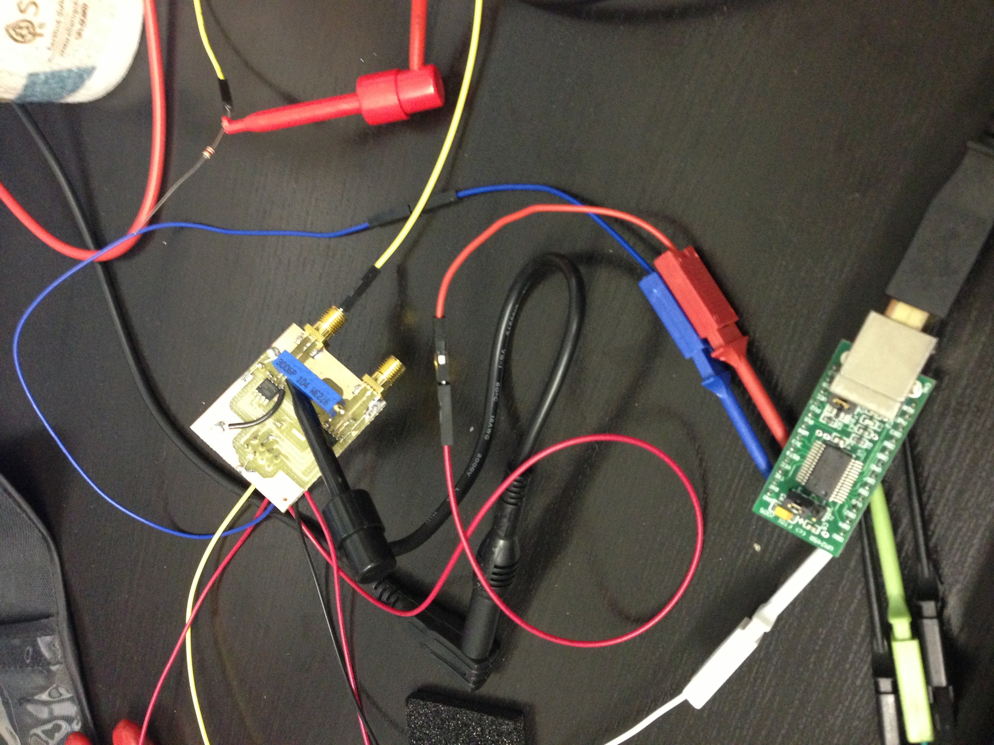
First, I made the dual DAC board with two MAX515's - simple, 10-bit, SPI DACs.
Aesthetically the board was not stunning - I used too large a drill for the through holes, and thus my pads were blown out. However, it was salavgable, so I continued putting it together and testing it by bit-banging the DACs with an FT245R dev board:
With that working well, I dead-bugged the modulator, a TRF370417 that will handle carrier freqs of 50 MHz through 6 GHz, to another board:

As pretty as that board turned out, it was unfortunately (and predictably) extremely noisy. Oh well, I suppose I will just have to make a proper board for all 3 chips...
First, I made the dual DAC board with two MAX515's - simple, 10-bit, SPI DACs.
Aesthetically the board was not stunning - I used too large a drill for the through holes, and thus my pads were blown out. However, it was salavgable, so I continued putting it together and testing it by bit-banging the DACs with an FT245R dev board:
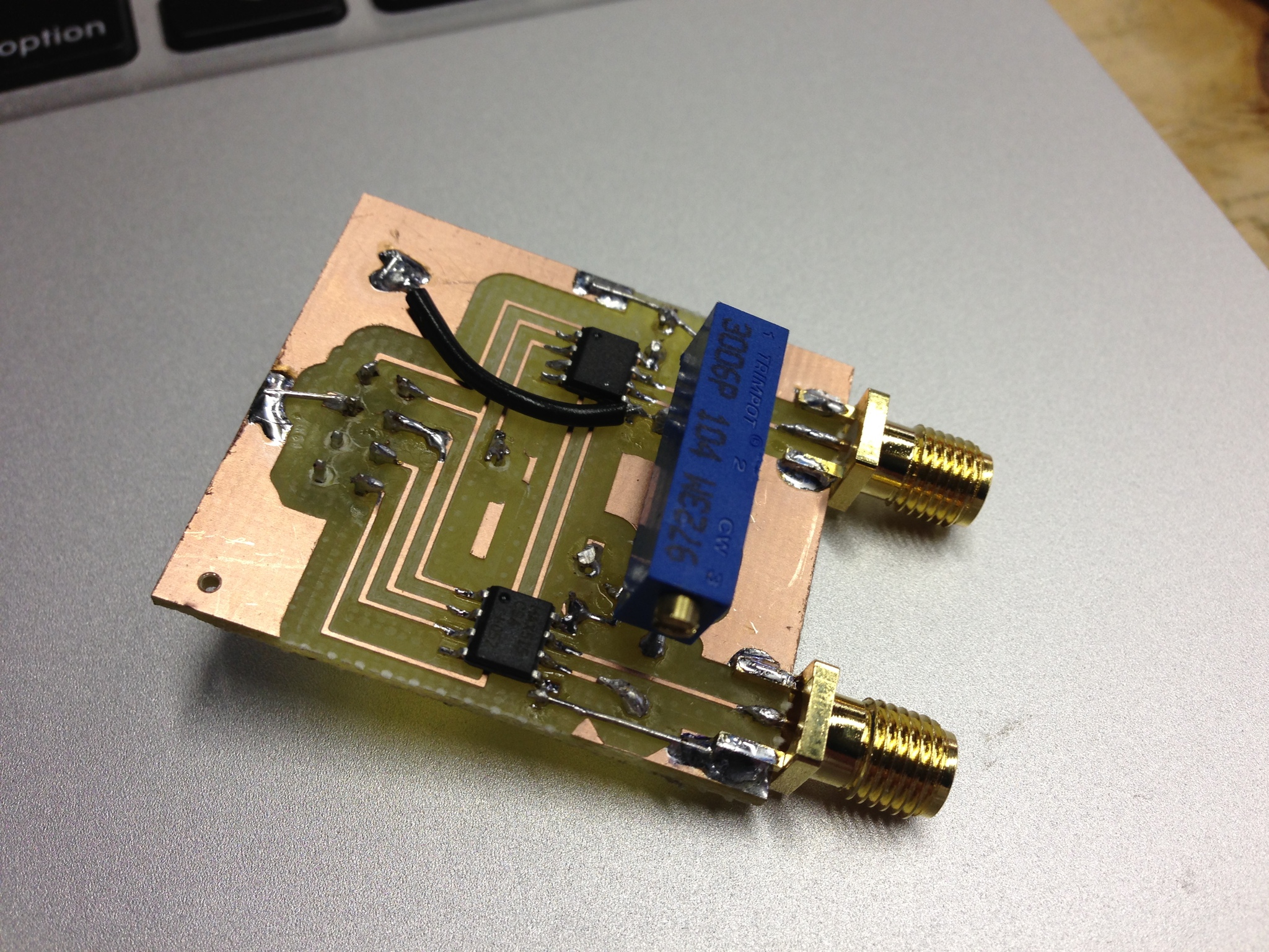
With that working well, I dead-bugged the modulator, a TRF370417 that will handle carrier freqs of 50 MHz through 6 GHz, to another board:
As pretty as that board turned out, it was unfortunately (and predictably) extremely noisy. Oh well, I suppose I will just have to make a proper board for all 3 chips...
Saturday, December 15. 2012
Reverse Engineering an Audi ECU
The thing that annoys me most about the ECU in my car is that it gives barely any debugging information about sensors and states. It's an older car so some of the sensors started getting a little wacky, but which ones? Fast forward a week and I had decided I needed to pull the code off the ECU to see how it works, then add a few functions of my own. There are a few businesses out there that reflash ECUs for performance increases and such, so if they can do it so can I.
I started by grabbing an ECU for my year and model of car from a junkyard, and opening it up.

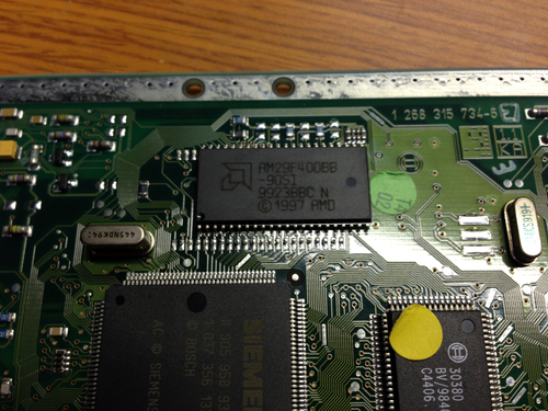
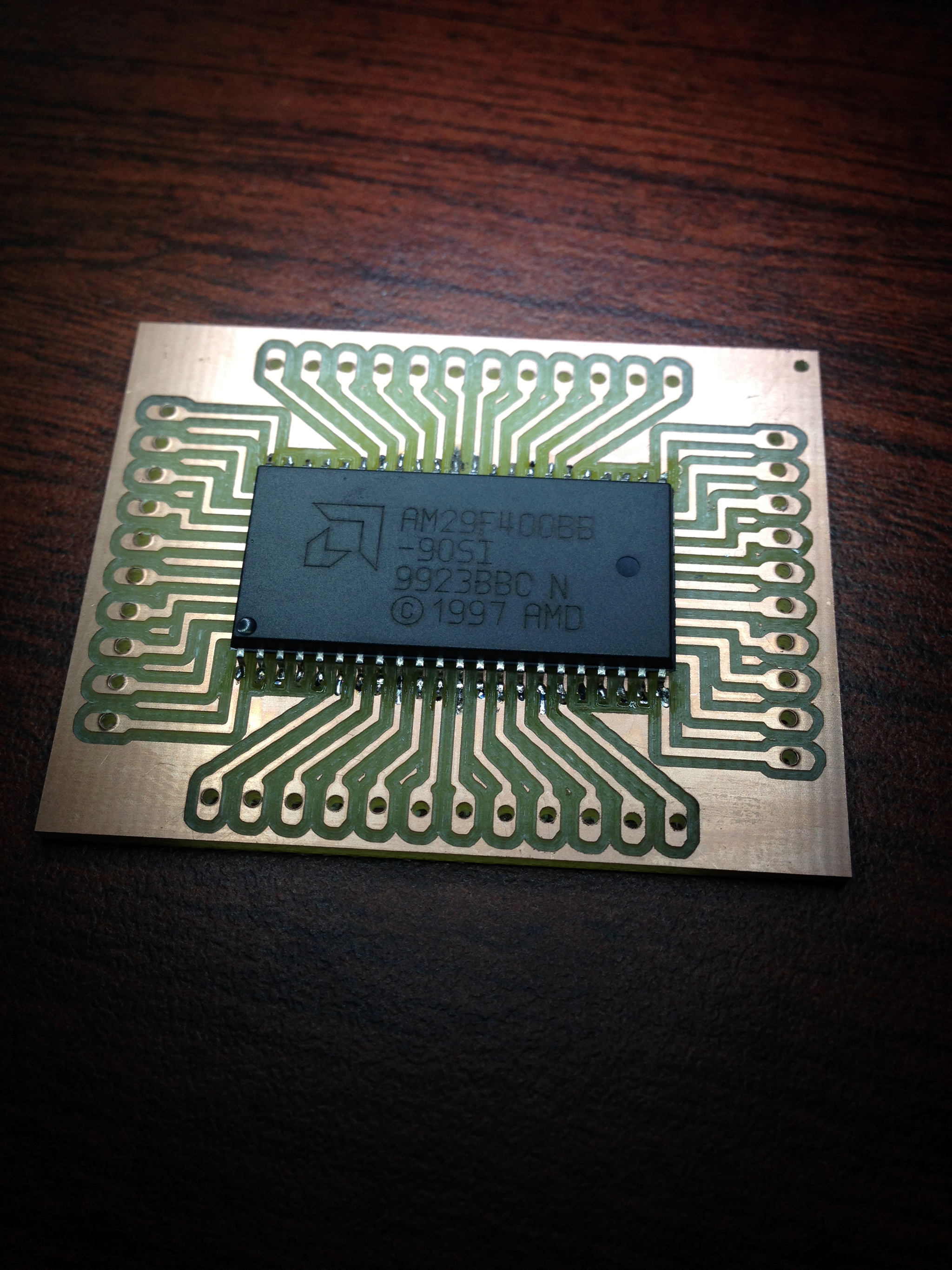
A quick glance shows that it's very simple: a C167 MCU, which loads its code from an Am29F400B flash at boot. The C167 is a great device for cars, as it has a ton of PWM channels and speaks CANBUS natively, and even includes the ability to load code via CANBUS. I was able to quickly find the datasheet and debugging hints documents, as well as a datasheet for the flash itself. Clearly, my next course of action was to yoink the flash and read it (note that in the above pics, I've already desoldered it from the board).
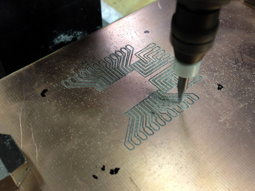
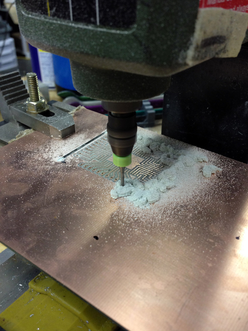
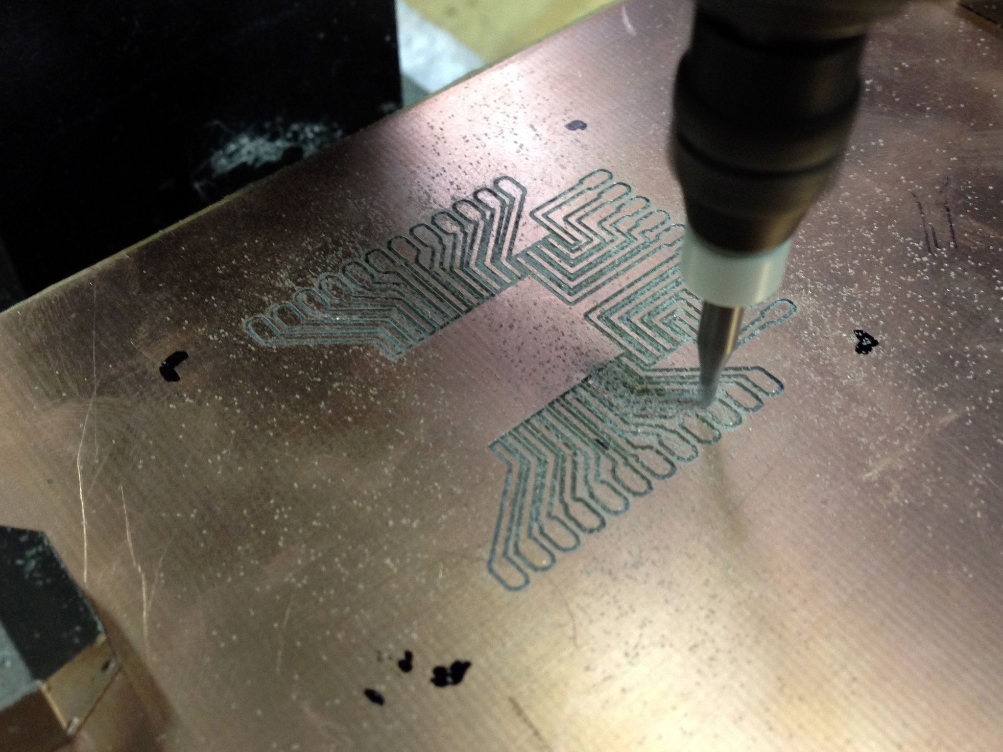
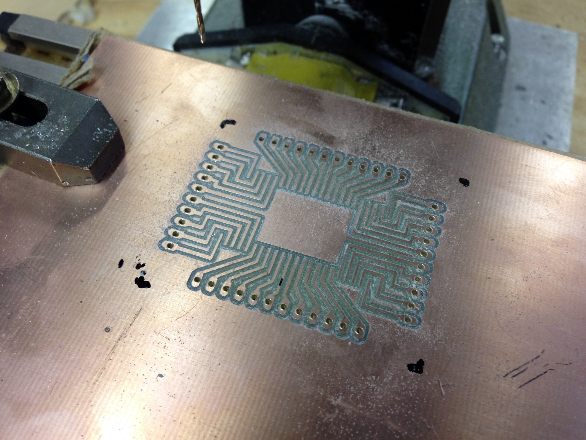
I hacked up a board design to give me easy access to the pins, and cut it using the mill:

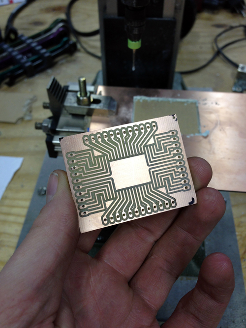
I did my math right and it came out great the first time. I had quite an internal debate about reading the data though- the elegant way to go about it would have been to write a general FPGA memory reader-writer that would also allow me to do passive memory snooping (ie, latch on address changes and record both the address and data value), but I decided to focus on one project at a time and just wrote a few lines of C for an Atmega board I had handy:

It worked nicely! I need to spend some time mapping out the IO addresses, but at first glance, the bootloader has an amusing tamper-protection scheme. The first block of code on the flash loads data into RAM from farther down the flash itself... but adds 1 to each value. Thus, to recover the original instructions, all I had to do was decrement each value by one and pass it into the disassembler again. Epic.
I started by grabbing an ECU for my year and model of car from a junkyard, and opening it up.
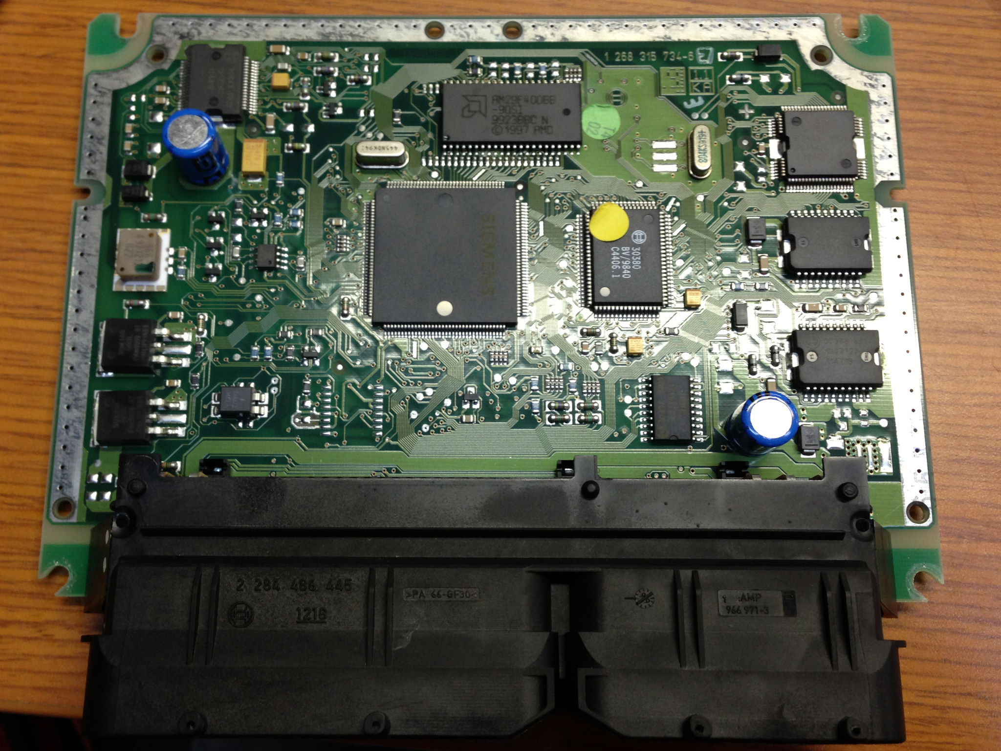
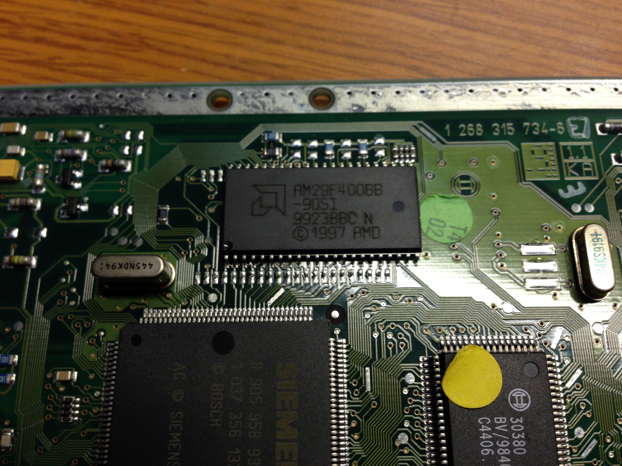
A quick glance shows that it's very simple: a C167 MCU, which loads its code from an Am29F400B flash at boot. The C167 is a great device for cars, as it has a ton of PWM channels and speaks CANBUS natively, and even includes the ability to load code via CANBUS. I was able to quickly find the datasheet and debugging hints documents, as well as a datasheet for the flash itself. Clearly, my next course of action was to yoink the flash and read it (note that in the above pics, I've already desoldered it from the board).
I hacked up a board design to give me easy access to the pins, and cut it using the mill:

I did my math right and it came out great the first time. I had quite an internal debate about reading the data though- the elegant way to go about it would have been to write a general FPGA memory reader-writer that would also allow me to do passive memory snooping (ie, latch on address changes and record both the address and data value), but I decided to focus on one project at a time and just wrote a few lines of C for an Atmega board I had handy:


It worked nicely! I need to spend some time mapping out the IO addresses, but at first glance, the bootloader has an amusing tamper-protection scheme. The first block of code on the flash loads data into RAM from farther down the flash itself... but adds 1 to each value. Thus, to recover the original instructions, all I had to do was decrement each value by one and pass it into the disassembler again. Epic.
Wednesday, November 21. 2012
Turbo Controller
My car, an Audi A4 1.8t, opens the wastegate at 8psi above atmospheric pressure, stock. Since clearly more power is better (and building stuff is entertaining), I needed to make something to adjust the boost setting.
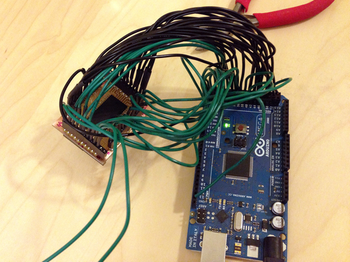
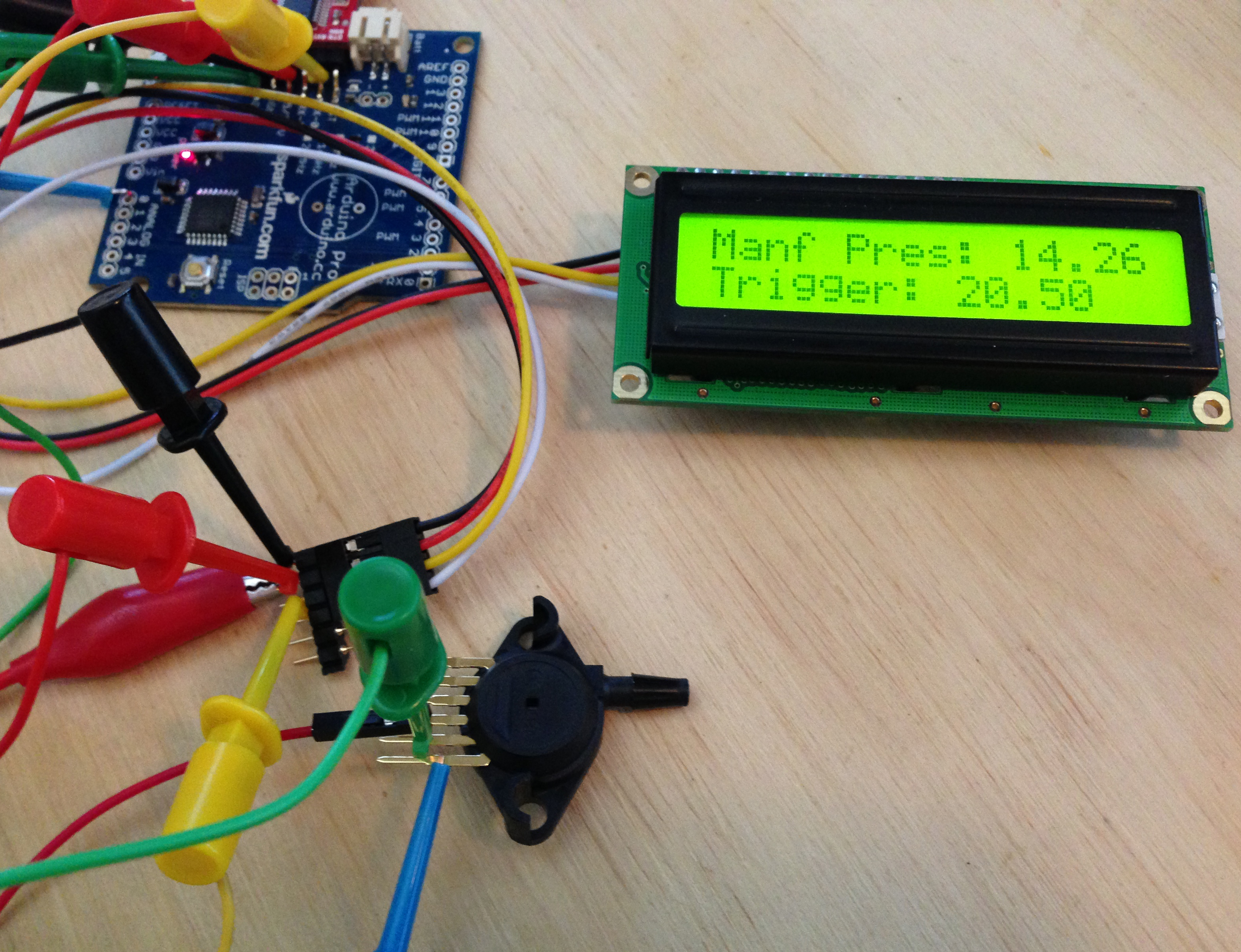
In standard turbocharger systems, there is simply a diaphragm that pops at the set pressure, and allows air to flow into the wastegate, reducing the amount of flow through the turbine, thus lowering the output pressure of the compressor. In the audi, there is a valve called the N75 with a two-conductor cable and 3 hoses connected to it: the turbo compressor tap, the wastegate input, and the airbox (for clean air feed under vacuum). I assumed this was simply a solenoid valve, and energizing it causes it to open. As such, my first code revision simply emulated a manual boost controller: at the set pressure (controlled by potentiometer), energize the valve and open the wastegate.

I hacked this all into the car in an evening with an arduino and an N-channel MOSFET (I KNEW that cat5 I ran into the engine compartment would come in handy...) and went for a spin. The results were... unexpected. The car drove just like it did normally and my manifold pressure gauge didn't register anything abnormal, except for one blip where the car unexpectedly made insane power while I was turning a corner. Hmmm.

I plugged the N75 back into the ECU and put my scope on it. Ah! It was being PWM'd!
It turns out the the N75 is actually a spring-controlled valve that begins releasing air at it's set pressure of 8psi over ambient. However, the solenoid coil in it can be pushed in either direction to lower or raise the setpoint. So, my logic was backwards: in order to make more boost, you energize the coil to push against the spring. I adjusted my code to PWM the coil, pushing hardest just above 8psi boost then tapering off to the setpoint for a smooth transition. It works great! The car makes significantly more power running 20psi of boost.
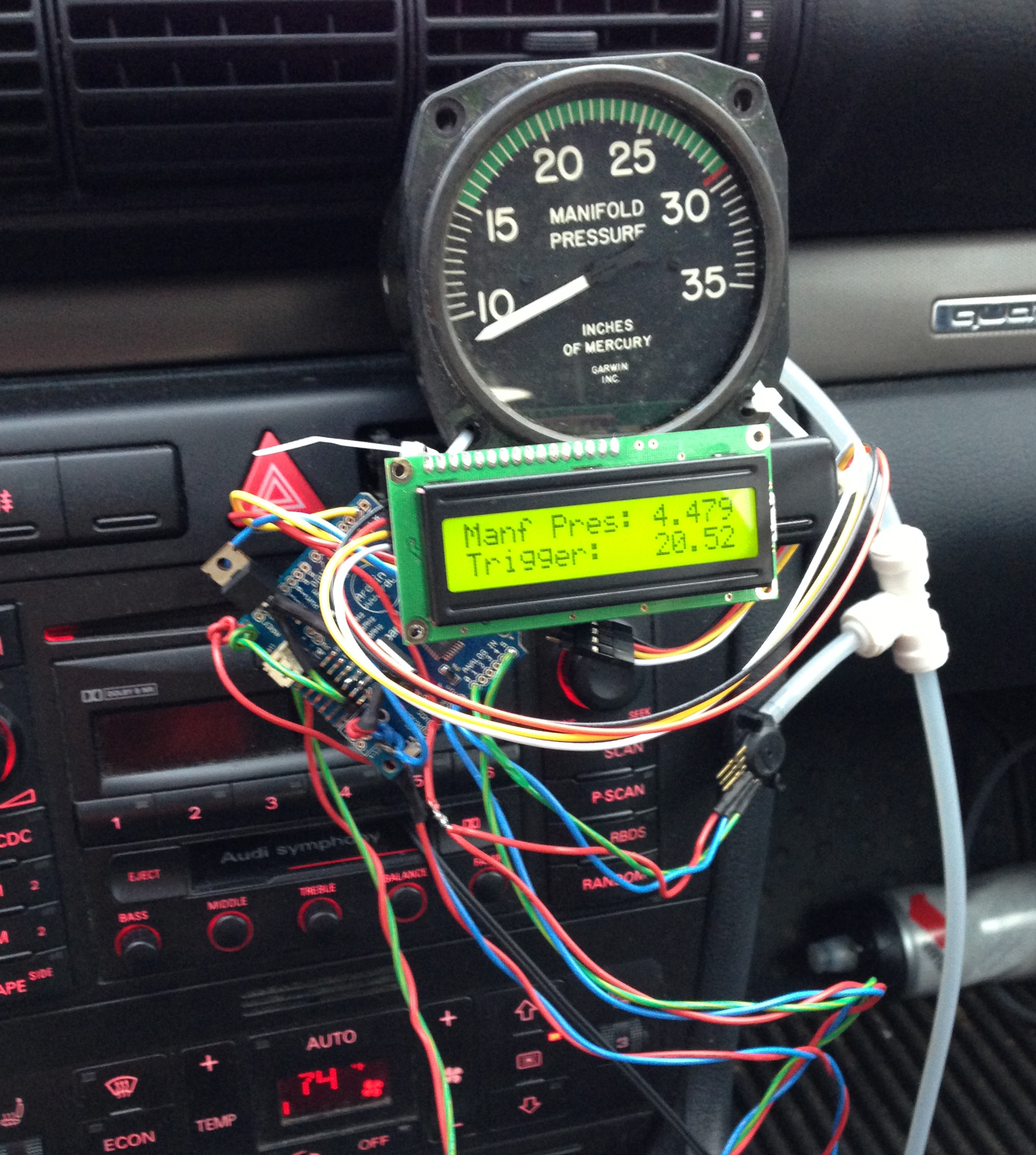
The only issue with that setup was the placement of my pressure transducer: I connected it to the tap from the intake manifold, post-throttle. This means that the turbo can be ramming out 30psi, but if the throttle is closed we still see vacuum. This wouldn't be a huge issue, except that the ECU's manifold pressure sensor is located pre-throttle, and it (a) sets the mixture and (b) cuts the injectors if it sees a dangerous level of boost (about 22psi). Whenever I would sharply accelerate or take my foot off the gas, the resulting spike from the throttle movement would send the pre-throttle pressure over that limit and cause the injectors to cut then surge back - not very great.
I have the system out of the car at the moment to install up front with the new pressure transducer placement just after the turbo. Should be splendid.
In standard turbocharger systems, there is simply a diaphragm that pops at the set pressure, and allows air to flow into the wastegate, reducing the amount of flow through the turbine, thus lowering the output pressure of the compressor. In the audi, there is a valve called the N75 with a two-conductor cable and 3 hoses connected to it: the turbo compressor tap, the wastegate input, and the airbox (for clean air feed under vacuum). I assumed this was simply a solenoid valve, and energizing it causes it to open. As such, my first code revision simply emulated a manual boost controller: at the set pressure (controlled by potentiometer), energize the valve and open the wastegate.
I hacked this all into the car in an evening with an arduino and an N-channel MOSFET (I KNEW that cat5 I ran into the engine compartment would come in handy...) and went for a spin. The results were... unexpected. The car drove just like it did normally and my manifold pressure gauge didn't register anything abnormal, except for one blip where the car unexpectedly made insane power while I was turning a corner. Hmmm.
I plugged the N75 back into the ECU and put my scope on it. Ah! It was being PWM'd!
It turns out the the N75 is actually a spring-controlled valve that begins releasing air at it's set pressure of 8psi over ambient. However, the solenoid coil in it can be pushed in either direction to lower or raise the setpoint. So, my logic was backwards: in order to make more boost, you energize the coil to push against the spring. I adjusted my code to PWM the coil, pushing hardest just above 8psi boost then tapering off to the setpoint for a smooth transition. It works great! The car makes significantly more power running 20psi of boost.
The only issue with that setup was the placement of my pressure transducer: I connected it to the tap from the intake manifold, post-throttle. This means that the turbo can be ramming out 30psi, but if the throttle is closed we still see vacuum. This wouldn't be a huge issue, except that the ECU's manifold pressure sensor is located pre-throttle, and it (a) sets the mixture and (b) cuts the injectors if it sees a dangerous level of boost (about 22psi). Whenever I would sharply accelerate or take my foot off the gas, the resulting spike from the throttle movement would send the pre-throttle pressure over that limit and cause the injectors to cut then surge back - not very great.
I have the system out of the car at the moment to install up front with the new pressure transducer placement just after the turbo. Should be splendid.
Wednesday, September 5. 2012
Embedded WiFi with an RN-XV
I picked up an RN-XV from Sparkfun to see what it would do. I didn't read the docs before I ordered, and I expected to be reading and writing registers and building my own packets. However, I was almost disappointed to learn how much functionality is supported within and how easy it is to get working.
The RN-XV is a carrier board for Roving Networks' RN-171 WiFi module. Since the XV is meant to be pin compatible with the Xbees which use an odd pin spacing, I also ordered an Xbee Explorer Regulated to make connections and power easy (the FTDI cables I have are logic 3.3v but 5v Vcc, so the regulator is needed).
I plugged TX to Din, RX to Dout, added power, and BAM! Blinky lights!
WiFly Ver 2.32, 02-13-2012 on RN-171
MAC Addr=00:06:66:72:20:58
Auto-Assoc roving1 chan=0 mode=NONE FAILED
Unfortunately, it didn't respond to my serial input. After a bunch of tracing and reading, it turns out that the Xbee board does logic level shifting with diodes. The Xbees's have pullup resistors in their Din pins, however the RN modules do not. After adding a 10k resistor from Vcc to Din, I was able to link it to my network and ping things first try.
CMD
<2.32> set wlan phrase myWifiPasswd
AOK
<2.32> join mySSID
Auto-Assoc secure chan=11 mode=WPA1 SCAN OK
Joining mySSID now..
<2.32> Associated!
DHCP: Start
DHCP in 775ms, lease=86400s
IF=UP
DHCP=ON
IP=192.168.9.61:2000
NM=255.255.255.0
GW=192.168.9.1
Listen on 2000
ping 4.2.2.1
Ping try 4.2.2.1
<2.32> 64 bytes from 4.2.2.1: seq=1 ttl=251 time=6.56 ms
64 bytes from 4.2.2.1: seq=2 ttl=251 time=6.41 ms
<2.32>
With the default settings, you can open a socket to the device via wifi on port 2000. Any data that arrives goes out the serial, and any data in the serial goes out the socket. Easy as pie. Now I just need to find something cool to do with it...
For the curious: RN-XV Datasheet (pinout), RN-171 Manual and Command Set
Sunday, April 8. 2007
Current Happenings
Saturday, November 12. 2005
Logic Probe
I built an interface to the parallel port for use as a logic probe. I found this program that, using its own port driver, can sample the port at up to 1MHz, on 8 channels.
I built a pretty interface into a box with switches for the ground bus, plus I made some 2 conductor probes and some singlle conductor probes. Unfortunatly I couldn’t find any of those handy circuit clips, so I just have lame aligator clips on the probes.
While looking for something to actually do with the probe, I built a simple square wave oscillator with an LM555 timer. It was almost cool… and everything is cooler when it goes faster. So I started messing with the circuit to make it go as fast as possible. I don’t have very small capacitors, but with what I had I got the thing to 675.68 kHz. I think that’s pretty good. I poked around and got it to go a little faster, but at that point the probe began aliasing because it couldn’t sample any faster, so I couldn’t test how fast it was going.
I’m going to try to use this to reverse engeneer chips, ie monitor the memory bus and see what a particular chip is doing, but with only 8 channels and up to 1 mHz (usually about 800 kHz) it’s unlikely that I’ll find something simple enough to use it on. But hey, maybe I can still get linux on my toaster.
Saturday, November 6. 2004
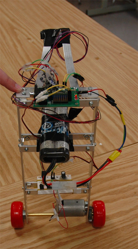
The Balancing Bot
I was looking around for a new project one day, when nBot caught my attention. I knew that balancing robots were hard (look how much the segway costs!), but the more I thought, the more I knew I had to try. [pics missing]
I am yet to have it balance indefinatly, at which point I will write a whole paper about doing this. However right now, I will just list the various versions, and how well they worked.
Version 1
This was (obviously) the first version. It was about 4 feet tall. I found that my motors move way too slowly to keep a bot this size up. Thus we went to the next version.
Version 2
I chopped off about a foot and a half, so the bot is now 2 and a half feet. I figured that the bot would be able to right itself better since the moment arm is shorter, thus the same linear speed is a much faster angular speed. It now stands for about 10 seconds, but inevitably still falls.
Version 2.5
I found that the problems were due to inaccurate readings in the IR sensors. So I made a running array of the last 8 values, and used the average of them for the calulation. This didn’t quite work, either. Look at these graphs:
For both of these tests, the IR sensor was stationary in a vise pointed at a wall. That should give you some idead how inaccurate it is. The first is without my fix:
And with the fix:
Version 3
I gave up on the IR sensors: now I’m using sonar. It’s much more accurate, but I only have one. So the bot now balances for about 20 seconds, but the wheels simply can’t go fast enough to catch up if it gets moving more than a few inches per second. I hope to make some new wheels today.
Version 3.1
I ran over to the wood shop (we don’t have a metal shop) and made some bigger wheels… it seemed to me that the servos had quite a bit of torque, but didn’t go fast enough. Thus, increase the radius, we increase the distance traveled per revolution.
Version 4.0
The whole bot has been completly redesigned. The wheels of wood were not prefectly true, and thus wobbled way too much to balance properly. Also, the body was not ideal, the motors weren’t good enough, it was too tall, heavy in the wrong places….
This new bot has been designed completly in aluminum. (And crafted with nothing more than a jigsaw and a drill, plus some Erector set peices.) Yet still, it’s nicer than the previous models. It balanced nicely, has a large electric drill motor and sonar.
I am yet to have it balance indefinatly, at which point I will write a whole paper about doing this. However right now, I will just list the various versions, and how well they worked.
Version 1


This was (obviously) the first version. It was about 4 feet tall. I found that my motors move way too slowly to keep a bot this size up. Thus we went to the next version.
Version 2
I chopped off about a foot and a half, so the bot is now 2 and a half feet. I figured that the bot would be able to right itself better since the moment arm is shorter, thus the same linear speed is a much faster angular speed. It now stands for about 10 seconds, but inevitably still falls.
Version 2.5
I found that the problems were due to inaccurate readings in the IR sensors. So I made a running array of the last 8 values, and used the average of them for the calulation. This didn’t quite work, either. Look at these graphs:
For both of these tests, the IR sensor was stationary in a vise pointed at a wall. That should give you some idead how inaccurate it is. The first is without my fix:
And with the fix:
Version 3
I gave up on the IR sensors: now I’m using sonar. It’s much more accurate, but I only have one. So the bot now balances for about 20 seconds, but the wheels simply can’t go fast enough to catch up if it gets moving more than a few inches per second. I hope to make some new wheels today.
Version 3.1
I ran over to the wood shop (we don’t have a metal shop) and made some bigger wheels… it seemed to me that the servos had quite a bit of torque, but didn’t go fast enough. Thus, increase the radius, we increase the distance traveled per revolution.
Version 4.0
The whole bot has been completly redesigned. The wheels of wood were not prefectly true, and thus wobbled way too much to balance properly. Also, the body was not ideal, the motors weren’t good enough, it was too tall, heavy in the wrong places….
This new bot has been designed completly in aluminum. (And crafted with nothing more than a jigsaw and a drill, plus some Erector set peices.) Yet still, it’s nicer than the previous models. It balanced nicely, has a large electric drill motor and sonar.
Email me:
jack {@} crepinc.com
Recent Projects:
Analog HF Transmitter
Audi ECU Reverse Engineering
Dual DAC QAM Modulator
FPGA QAM Modulator
Geiger Counter
Gyro-Stabilized DSLR Platform
Hybrid Rocket Engines
Turbocharger Controller
WWVB Rx and Tx
Older Projects:
Balancing Bot
Capacitor Array
CNC Mill
DCIR Renderer
Electric Gokart
Hovercraft
Low Alt. Temp. Model
Shopping Cart Locker
Trebuchet
My Twitter occasionally shows projects I'm working on.
My GitHub has code from a few projects on it.