Wednesday, May 14. 2014
Interfacing Cirrus Logic Audio ADCs
I've been considering ideas for audio gear of various sorts over the past few months, and decided a good starting place would be a solid ADC interface from which I could prototype concepts. Lots of companies make audio converters, but I settled on two models from Cirrus Logic: the CS5361 and CS5340. They are, respectively, balanced and unbalanced two-channel 24-bit 192 khz high dynamic range delta-sigma oversampling devices.
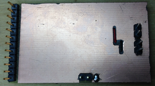
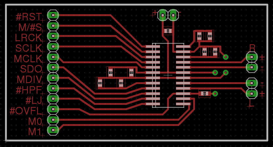
I started by laying out a super-simple protoboard for the CS5361. Since I wanted this to be quick and easy to cut on the CNC mill, the board is single-sided with the bare minimum of filtering, and without standard mixed signal board design concepts like separate analog and digital ground planes. While this will negatively affect the noise figure a bit, I wanted to get the device up and running with the minimum investment of time in case my assumptions regarding its usage and support were incorrect.

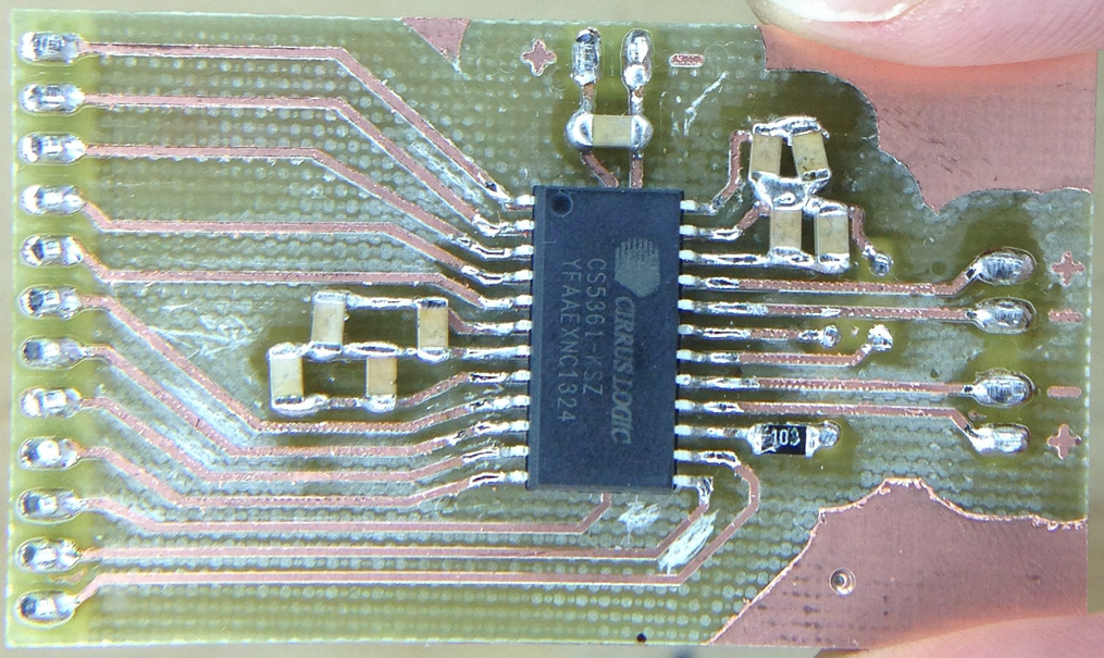
By the time I had finished the layout and cut the board, the samples order had arrived! Soldering was quick though a tad arduous - I need to use a larger 1206 footprint next time.

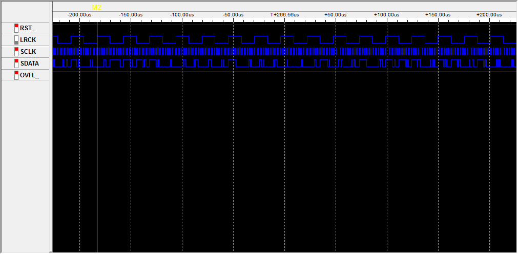
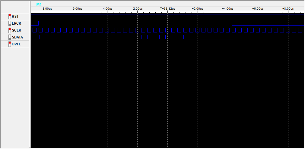
My ugly solder job notwithstanding, I plugged the unit into a breadboard, wired up an oscillator, config pins, and the logic analyzer, and was immediately rewarded with correct operation:
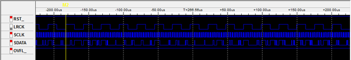
In short, by simply applying power, config pin states, and a master clock, the device will shift out ADC values (in 2's compliment form) msb-first on the falling edge of SCLK (ie, we sample on the rising edge):

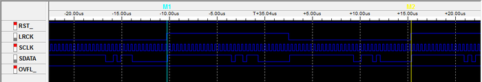
The only other line we need to worry about is LRCK, which indicates the channel being sent - you can see here that we get a left sample, then a right sample, then repeat:
With the hardware working, I set about writing the Verilog modules to nab samples from the ADC and send them off via USB (using an FT245R FIFO interface I have on hand). The code is extremely simple: on the rising edge of SCLK, samples are shifted into an 8-bit register - the size of the data bus on the USB interface. Every 8 bits, that register is strobed into the FT245R and the process repeats.
Byte alignment is provided by LRCK: on a start or reset condition from the USB host, the FPGA waits for a rising edge of LRCK before beginning the sampling and transmission of samples. This allows the client end to interpret the data stream without framing bytes: incoming data is simply shifted into 3-byte (24-bit) samples, left then right, and processed as desired.
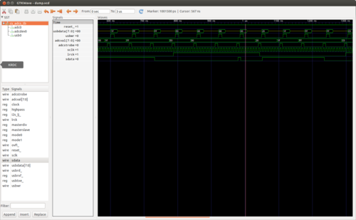
The code was quick to write and simulate with my favorite tools, iVerilog and GTKWave. I implemented a quick CS5361 module whose left and right channels count up and down (respectively) so as to simulate the rest of the pieces. Unfortunately I spent almost as much time debugging the code in hardware with the logic analyzer as I did writing the code, as Quartus (the Altera design software) is rather inconsistent in its handling of constants and register widths. (note: always read every line of output from the Altera synthesis toolchain - one can easily spend 4 hours trying to debug a problem that makes no sense only to find that the synthesis tool decided a constant was the wrong size and used zero instead)
In any event, I did manage to squash the few Quartus oddities that had caused the hardware to operate differently from the simulated code, and verified that the USB interface looked correct using the logic analyzer. Time for more spaghetti:
Time to test it out. In its current state, the FPGA will assert a reset condition on any received byte from the FIFO buffer. So, we will send a reset byte then read 24 samples of 6 bytes (3 for each channel):
root@ichor ~ # echo -n 0 > /dev/ttyUSB0 && dd if=/dev/ttyUSB0 count=24 bs=6 2>/dev/null | hexdump
0000000 3238 a13f 4a68 a650 0344 bd41 6632 ceaa
0000010 78f2 28f8 9764 19ca 7185 45b4 6bfd eabf
0000020 9825 8050 65e5 6122 3adc 0830 28f0 9dfc
0000030 d026 746a e2c0 befa 57dc 1fa4 4225 7b82
0000040 a61b ed00 2320 d641 e111 b648 a2f3 8d3a
0000050 bdfb afb6 1287 5963 ff57 9c8e 63a1 3971
0000060 4bfe ac6e 5081 9fae 2b0d 5c4c 6eaa 26b7
0000070 164b 6093 8378 96d8 138c 160e e661 a81b
0000080 81bc bdae 530b ec79 3537 6ada b0cc 4773
0000090
Success! With that working, the next steps are to implement the CS5340 and add proper dynamic configuration loading. From there, I am hoping to implement ADAT input and output and a simple device driver to interface the kernel audio subsystem.
I've put the code, board design, and a bit of documentation on GitHub: jackcarrozzo/cs_adcs.
I started by laying out a super-simple protoboard for the CS5361. Since I wanted this to be quick and easy to cut on the CNC mill, the board is single-sided with the bare minimum of filtering, and without standard mixed signal board design concepts like separate analog and digital ground planes. While this will negatively affect the noise figure a bit, I wanted to get the device up and running with the minimum investment of time in case my assumptions regarding its usage and support were incorrect.
By the time I had finished the layout and cut the board, the samples order had arrived! Soldering was quick though a tad arduous - I need to use a larger 1206 footprint next time.

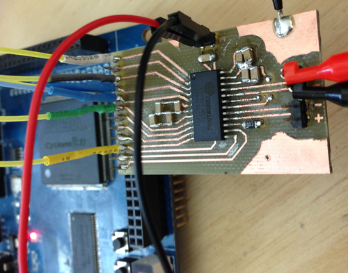
My ugly solder job notwithstanding, I plugged the unit into a breadboard, wired up an oscillator, config pins, and the logic analyzer, and was immediately rewarded with correct operation:
In short, by simply applying power, config pin states, and a master clock, the device will shift out ADC values (in 2's compliment form) msb-first on the falling edge of SCLK (ie, we sample on the rising edge):
The only other line we need to worry about is LRCK, which indicates the channel being sent - you can see here that we get a left sample, then a right sample, then repeat:

With the hardware working, I set about writing the Verilog modules to nab samples from the ADC and send them off via USB (using an FT245R FIFO interface I have on hand). The code is extremely simple: on the rising edge of SCLK, samples are shifted into an 8-bit register - the size of the data bus on the USB interface. Every 8 bits, that register is strobed into the FT245R and the process repeats.
Byte alignment is provided by LRCK: on a start or reset condition from the USB host, the FPGA waits for a rising edge of LRCK before beginning the sampling and transmission of samples. This allows the client end to interpret the data stream without framing bytes: incoming data is simply shifted into 3-byte (24-bit) samples, left then right, and processed as desired.

The code was quick to write and simulate with my favorite tools, iVerilog and GTKWave. I implemented a quick CS5361 module whose left and right channels count up and down (respectively) so as to simulate the rest of the pieces. Unfortunately I spent almost as much time debugging the code in hardware with the logic analyzer as I did writing the code, as Quartus (the Altera design software) is rather inconsistent in its handling of constants and register widths. (note: always read every line of output from the Altera synthesis toolchain - one can easily spend 4 hours trying to debug a problem that makes no sense only to find that the synthesis tool decided a constant was the wrong size and used zero instead)

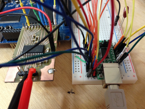
In any event, I did manage to squash the few Quartus oddities that had caused the hardware to operate differently from the simulated code, and verified that the USB interface looked correct using the logic analyzer. Time for more spaghetti:

Time to test it out. In its current state, the FPGA will assert a reset condition on any received byte from the FIFO buffer. So, we will send a reset byte then read 24 samples of 6 bytes (3 for each channel):
root@ichor ~ # echo -n 0 > /dev/ttyUSB0 && dd if=/dev/ttyUSB0 count=24 bs=6 2>/dev/null | hexdump
0000000 3238 a13f 4a68 a650 0344 bd41 6632 ceaa
0000010 78f2 28f8 9764 19ca 7185 45b4 6bfd eabf
0000020 9825 8050 65e5 6122 3adc 0830 28f0 9dfc
0000030 d026 746a e2c0 befa 57dc 1fa4 4225 7b82
0000040 a61b ed00 2320 d641 e111 b648 a2f3 8d3a
0000050 bdfb afb6 1287 5963 ff57 9c8e 63a1 3971
0000060 4bfe ac6e 5081 9fae 2b0d 5c4c 6eaa 26b7
0000070 164b 6093 8378 96d8 138c 160e e661 a81b
0000080 81bc bdae 530b ec79 3537 6ada b0cc 4773
0000090
Success! With that working, the next steps are to implement the CS5340 and add proper dynamic configuration loading. From there, I am hoping to implement ADAT input and output and a simple device driver to interface the kernel audio subsystem.
I've put the code, board design, and a bit of documentation on GitHub: jackcarrozzo/cs_adcs.
Trackbacks
Trackback specific URI for this entry
No Trackbacks
Email me:
jack {@} crepinc.com
Recent Projects:
Analog HF Transmitter
Audi ECU Reverse Engineering
Dual DAC QAM Modulator
FPGA QAM Modulator
Geiger Counter
Gyro-Stabilized DSLR Platform
Hybrid Rocket Engines
Turbocharger Controller
WWVB Rx and Tx
Older Projects:
Balancing Bot
Capacitor Array
CNC Mill
DCIR Renderer
Electric Gokart
Hovercraft
Low Alt. Temp. Model
Shopping Cart Locker
Trebuchet
My Twitter occasionally shows projects I'm working on.
My GitHub has code from a few projects on it.